
HGTECH 武汉华工激光工程责任有限公司 privacy policy
Copyright HGLaser Engineering Co,.Ltd. All Rights Reserver.
The rapid evolution of AI is no longer determined by computing chips alone. As large-scale AI models continue to expand, the ability to move massive volumes of data efficiently has become equally critical.
Since 2020, the computational workload required for large model training has increased by approximately 100 times. Meanwhile, xAI’s Colossus cluster has exceeded 100,000 GPUs, becoming one of the world’s largest AI computing clusters.
These developments reveal a fundamental reality:
AI performance is increasingly limited by data transmission capabilities.
According to TrendForce, the global AI optical transceiver market is projected to increase from USD 16.5 billion in 2025 to USD 26 billion in 2026, representing annual growth of more than 57%. LightCounting forecasts that the Ethernet optical module market will grow by 65% year over year in 2026, reaching USD 38 billion by 2028.
Driven by AI infrastructure expansion, optical communications are entering a new phase of rapid technological evolution.
In AI data centers, optical modules function like the “neural networks” connecting thousands of GPUs. Without high-speed optical communication, even the most powerful computing clusters cannot operate as a unified system.
Optical networking equipment already represents approximately 30–40% of total data center network investment, making optical module manufacturing capability a critical factor influencing AI infrastructure deployment.
The industry is rapidly advancing toward higher-speed optical connectivity:
However, achieving higher bandwidth, reliability, lower power consumption, and reduced latency requires breakthroughs not only in design but also in manufacturing.
For example, in 1.6T silicon photonics modules, optical coupling accuracy has improved from approximately ±5μm during the 400G era to ±0.5μm or below. Meanwhile, single-channel coupling time must be shortened to within 10 seconds, while maintaining flexible switching among multiple product models.
A single percentage-point improvement in coupling yield can translate into millions of RMB in annual savings for a production line with an annual output of 100,000 units.
A complete optical module production line generally includes 15–20 major process stations. Among these, optical coupling typically accounts for 30–40% of total production time, making it one of the biggest bottlenecks during capacity expansion.
For 1.6T silicon photonics fiber array (FA) coupling, positioning accuracy requirements have reached the nanometer scale (±20nm), far beyond the capability of manual manufacturing.
Meanwhile, the global optical module production capacity gap is expected to reach 20–30% by 2026.
Traditional manual and semi-automated production methods can no longer simultaneously meet the demands of:
As a result, intelligent manufacturing equipment has become a critical growth driver in the next stage of optical communication development.
Industry estimates indicate that the global optical module manufacturing equipment market will exceed USD 5 billion in 2026, with annual growth exceeding 30%.
At the same time, technological transitions are accelerating:
Companies including Cisco and Intel have already introduced CPO prototype solutions. CPO technology can reduce power consumption of 800G ports from 14–16W to 5.2–5.6W.
However, emerging requirements such as nanometer-level silicon photonics-to-fiber array alignment and heterogeneous multi-chip integration have made traditional standalone automation insufficient.
The industry urgently requires integrated manufacturing platforms capable of supporting the next generation of optical module production.
With more than a decade of expertise in laser processing, precision motion control, and measurement technologies, HGLaser provides full-stack intelligent manufacturing solutions for AI optical module production.
Through proprietary technologies including:
HGLaser focuses on critical manufacturing stages including:
The company delivers intelligent equipment and complete production line solutions designed to help customers achieve stable and scalable mass production.
For 1.6T silicon photonics fiber array (FA) coupling, HGLaser achieves:
These capabilities enable high-precision alignment required for next-generation optical modules.
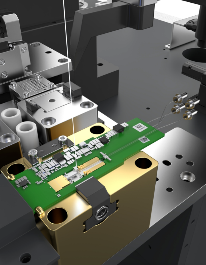
HGLaser’s assembly solutions address major manufacturing challenges, including:
These solutions have already been implemented in key production processes for multiple leading customers.
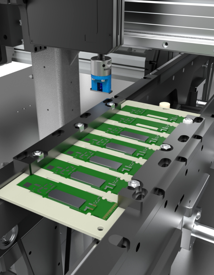
HGLaser’s intelligent inspection solutions provide:
This enables continuous improvement of production quality and manufacturing reliability.
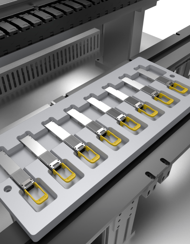
HGLaser is more than an intelligent equipment supplier. By focusing on real production challenges, the company builds integrated solutions covering:
Coupling → Assembly → Inspection → Complete Production Lines
From individual equipment to complete manufacturing systems, from process optimization to data-driven production management, HGLaser supports the evolution of optical communications from:
800G → 1.6T → 3.2T
Helping the global AI infrastructure industry achieve:
As AI continues to redefine computing boundaries, optical modules are reshaping the limits of data transmission.
And HGLaser is advancing the boundaries of optical module mass production.

