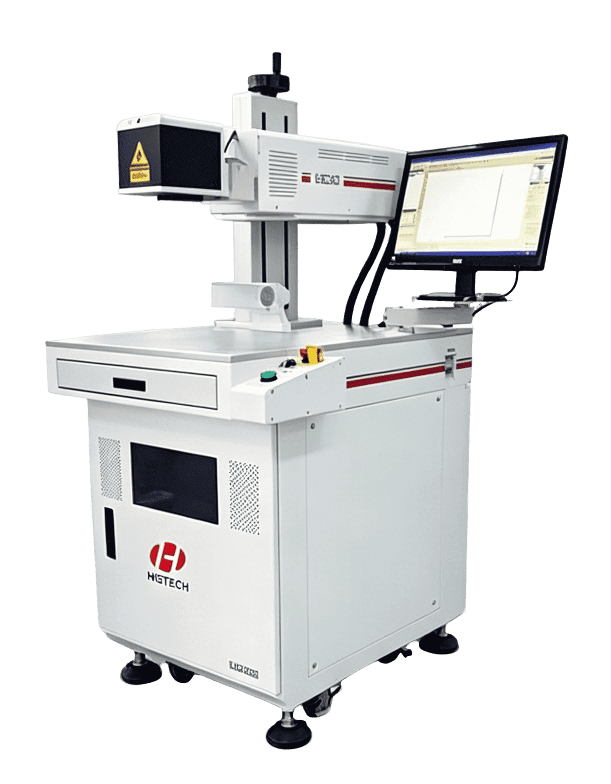
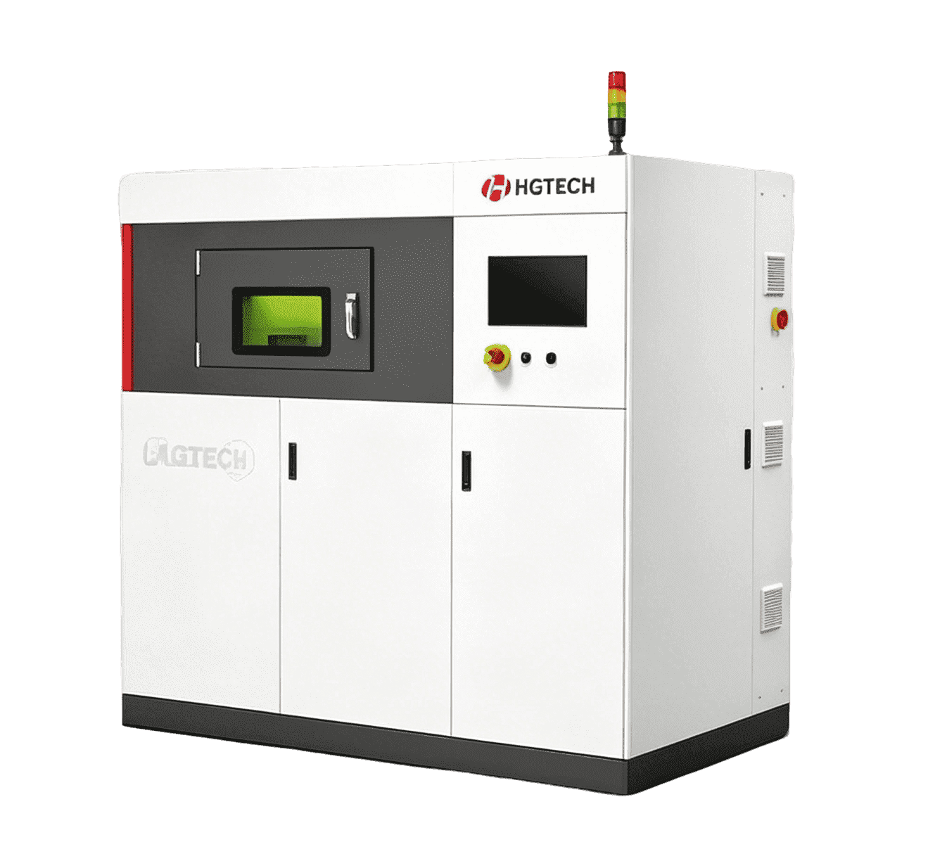
Automobile Industry
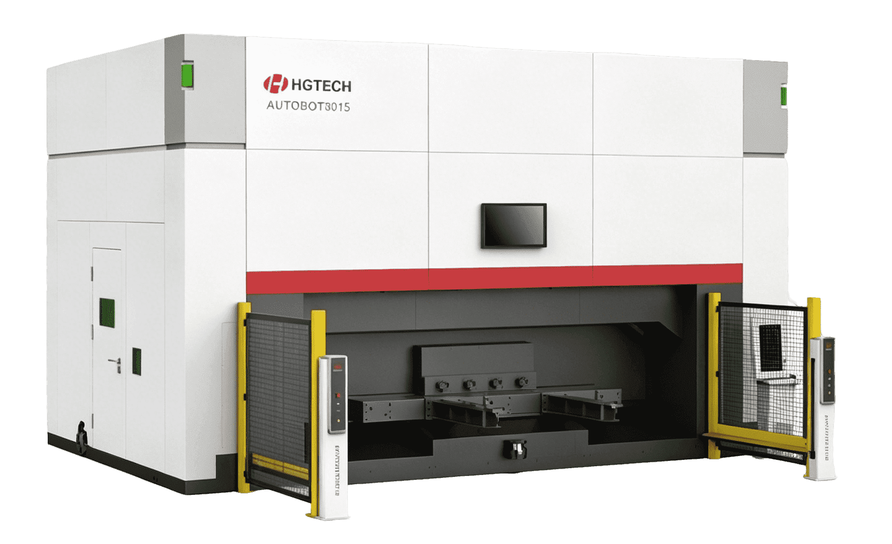
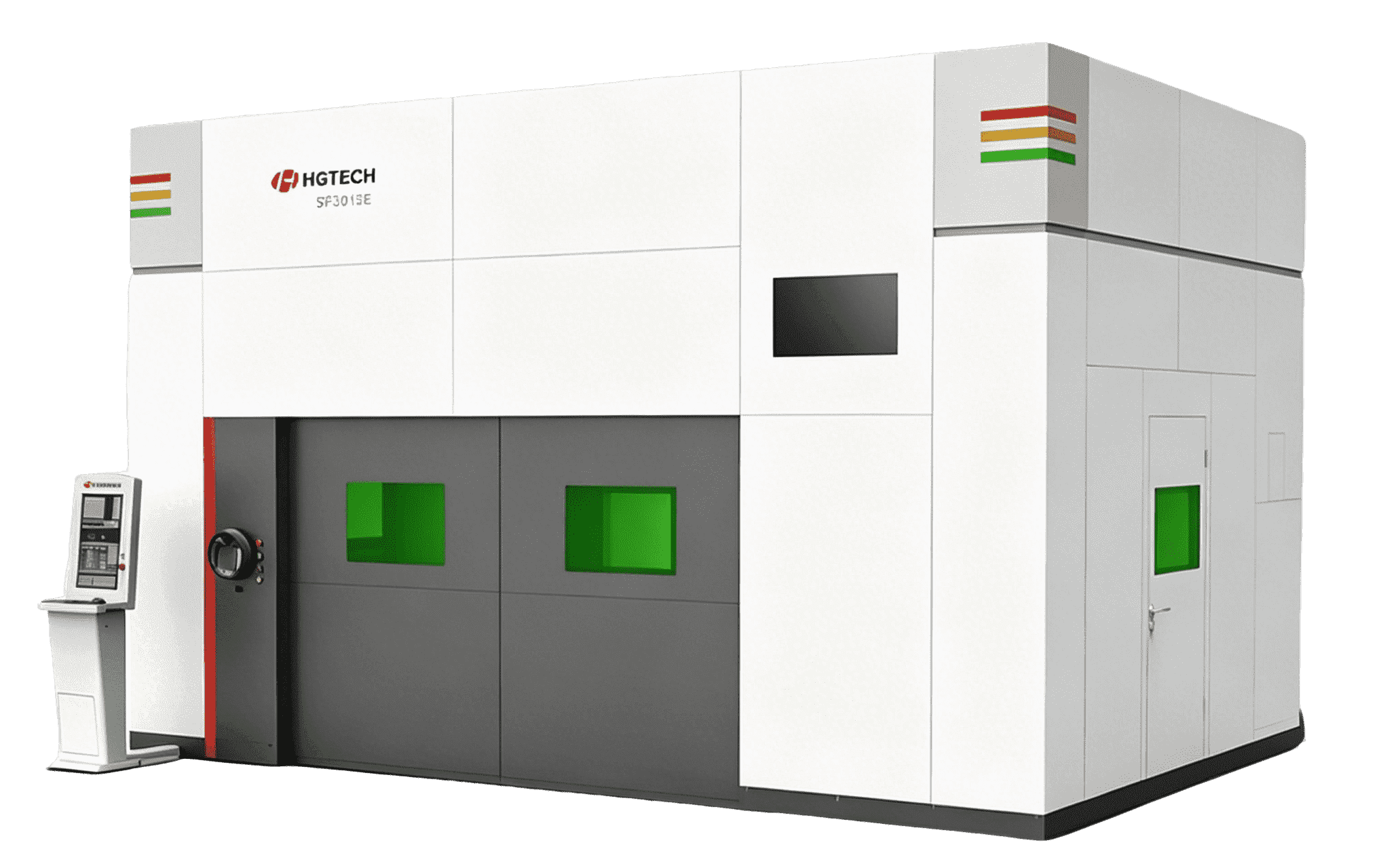
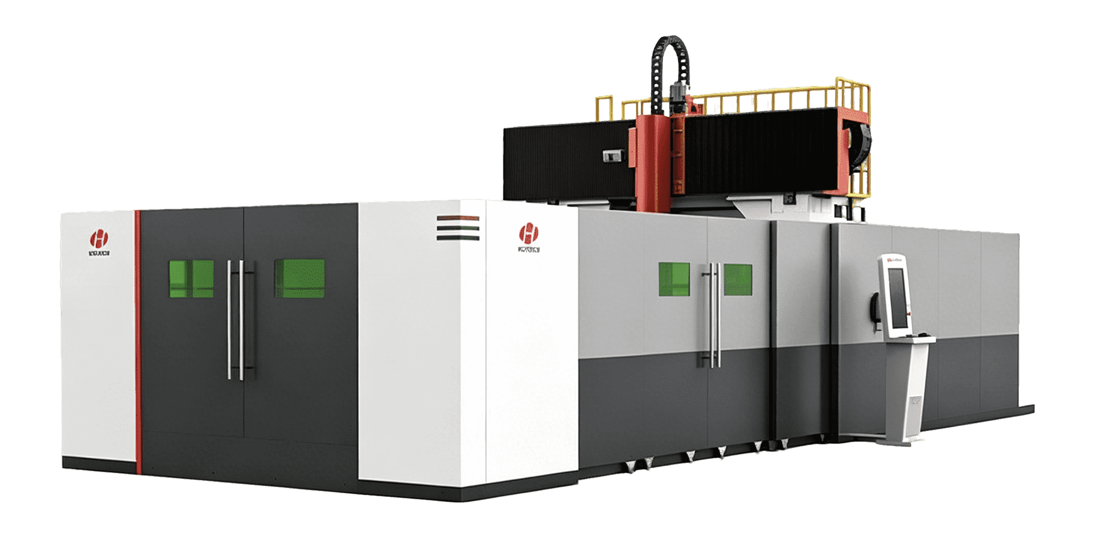
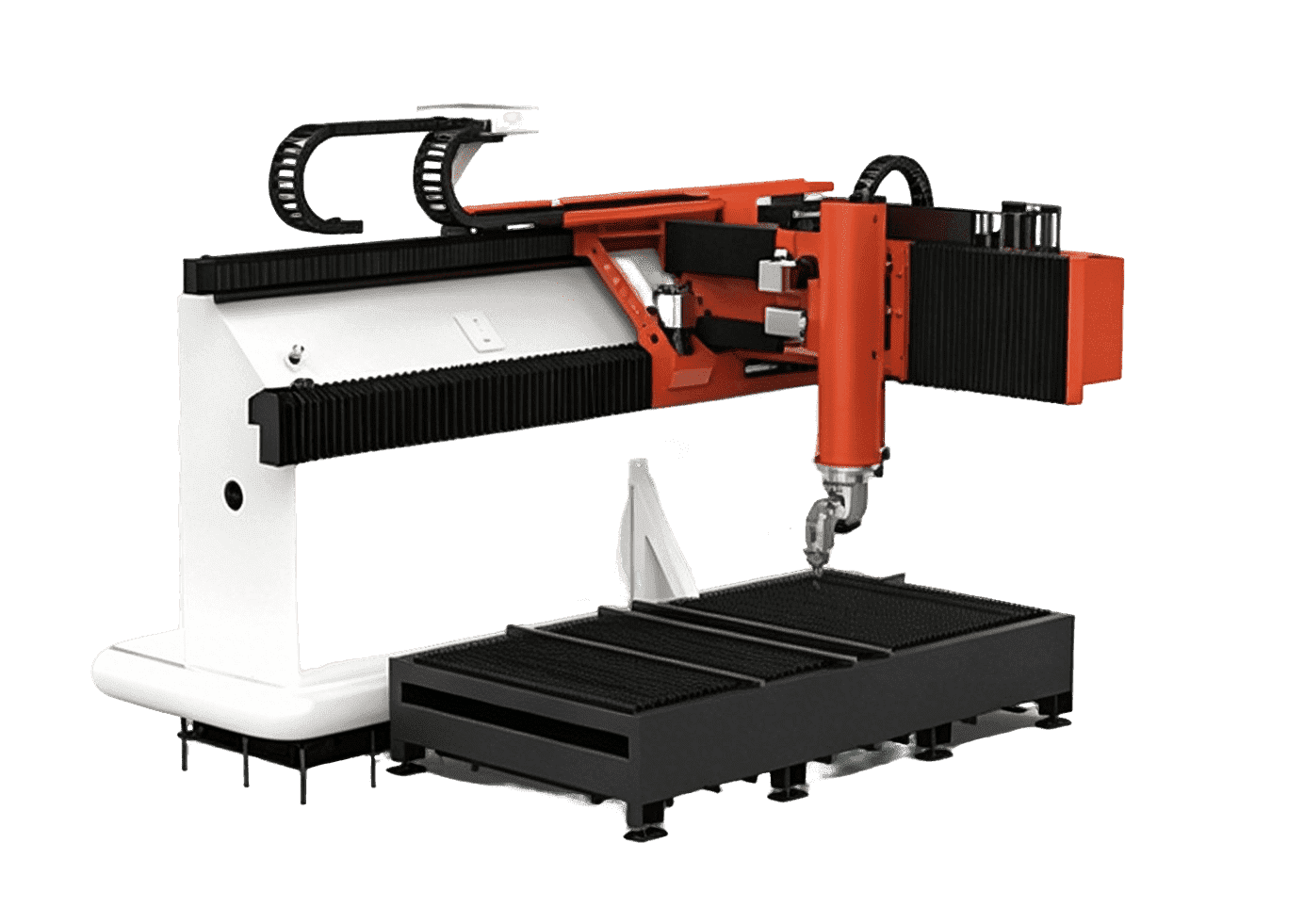
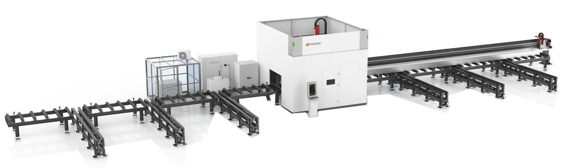
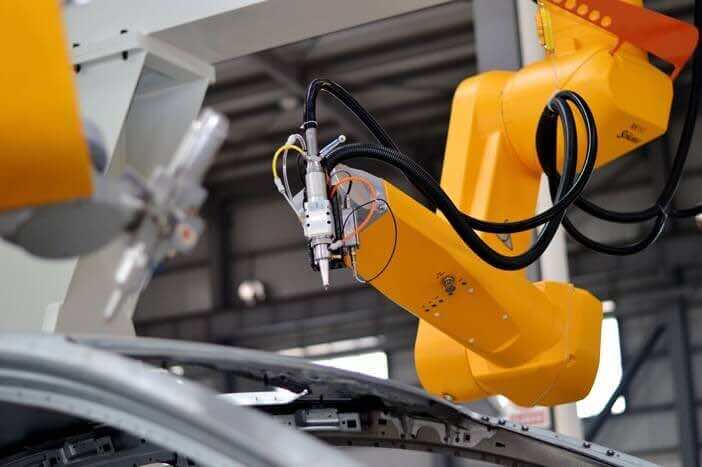
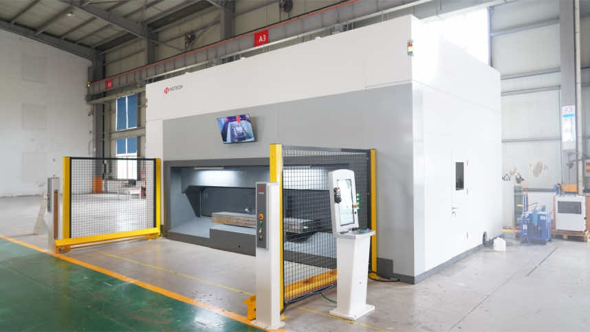
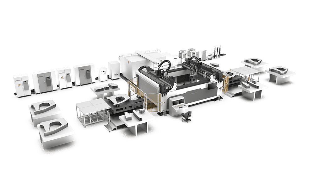
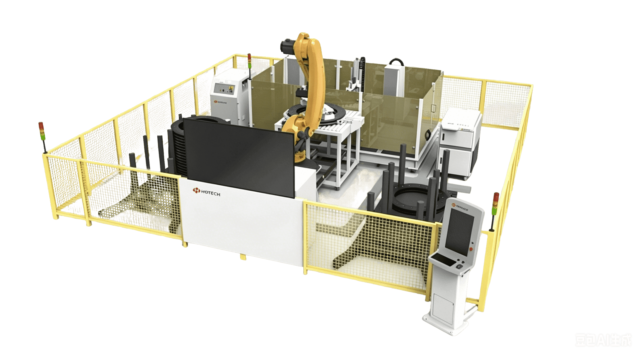
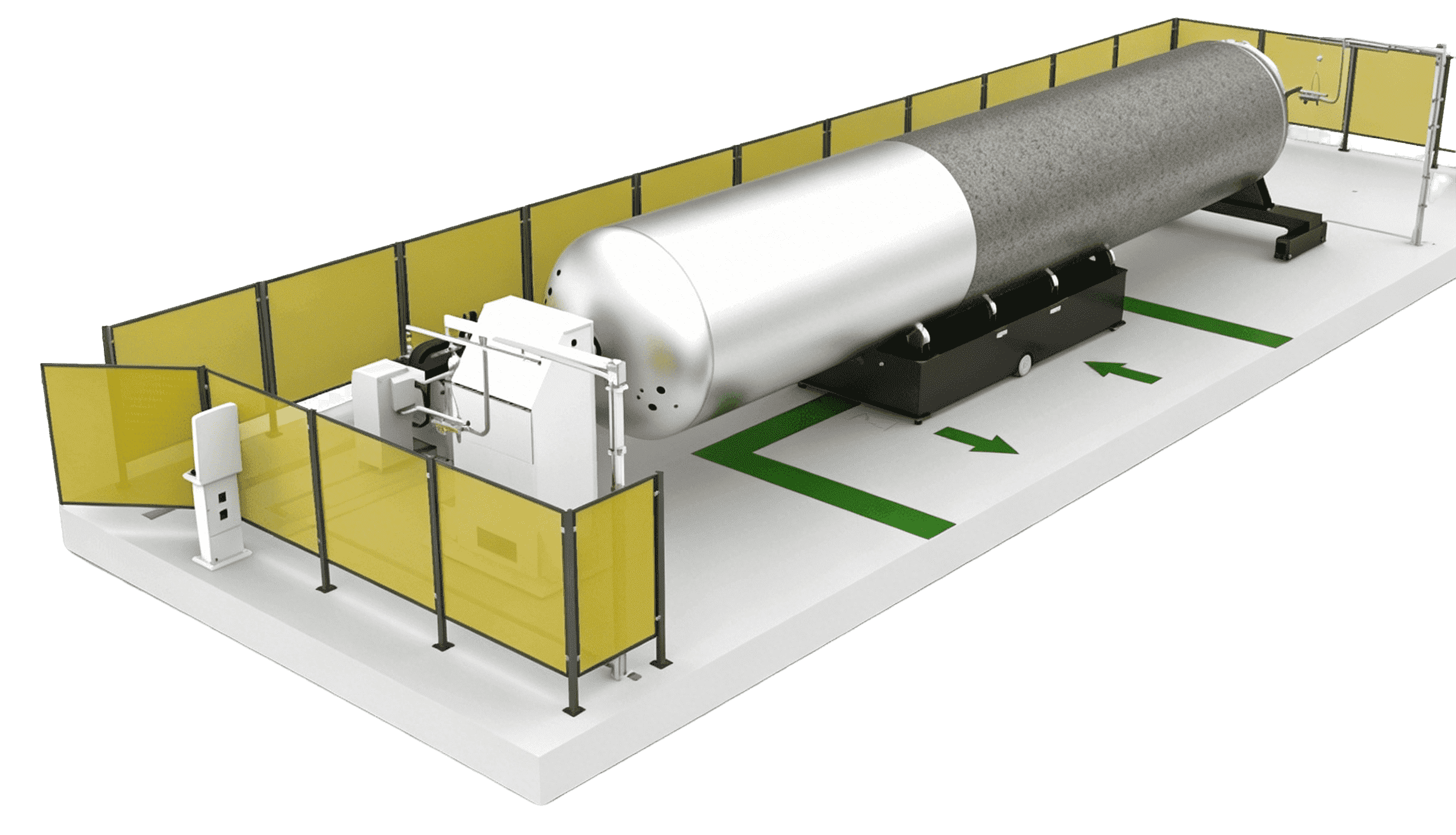
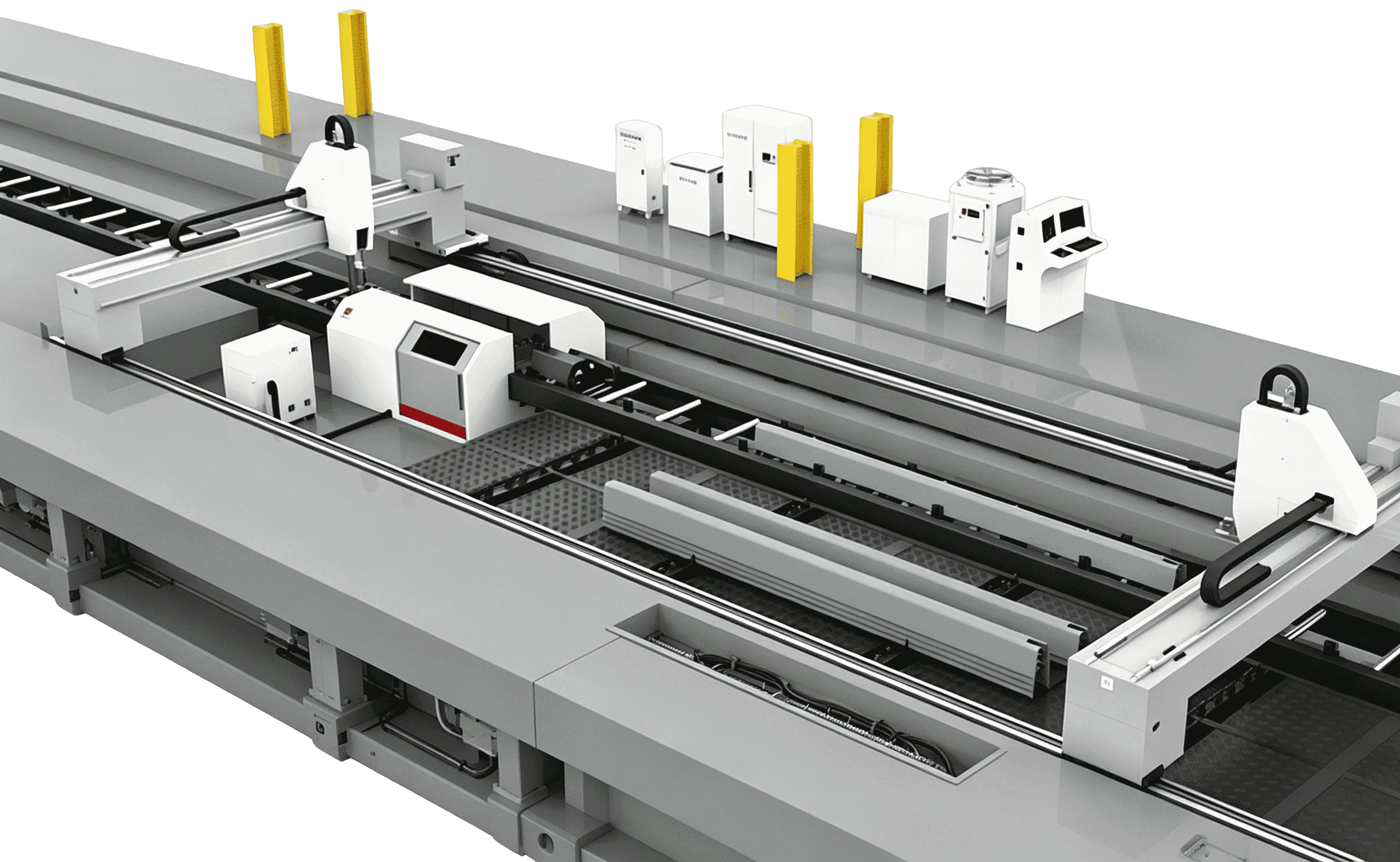
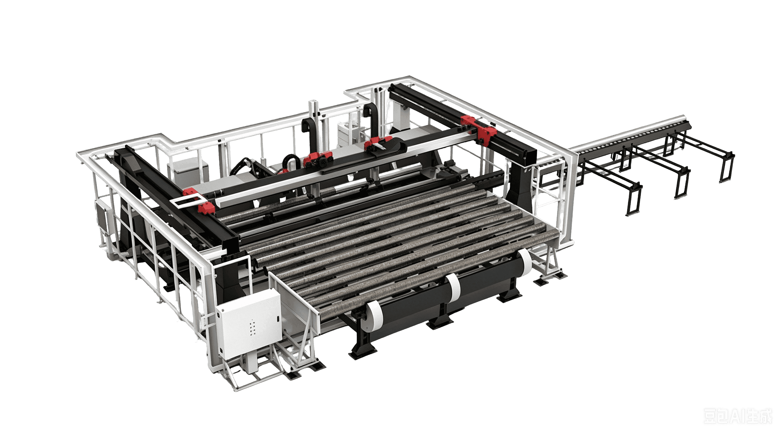
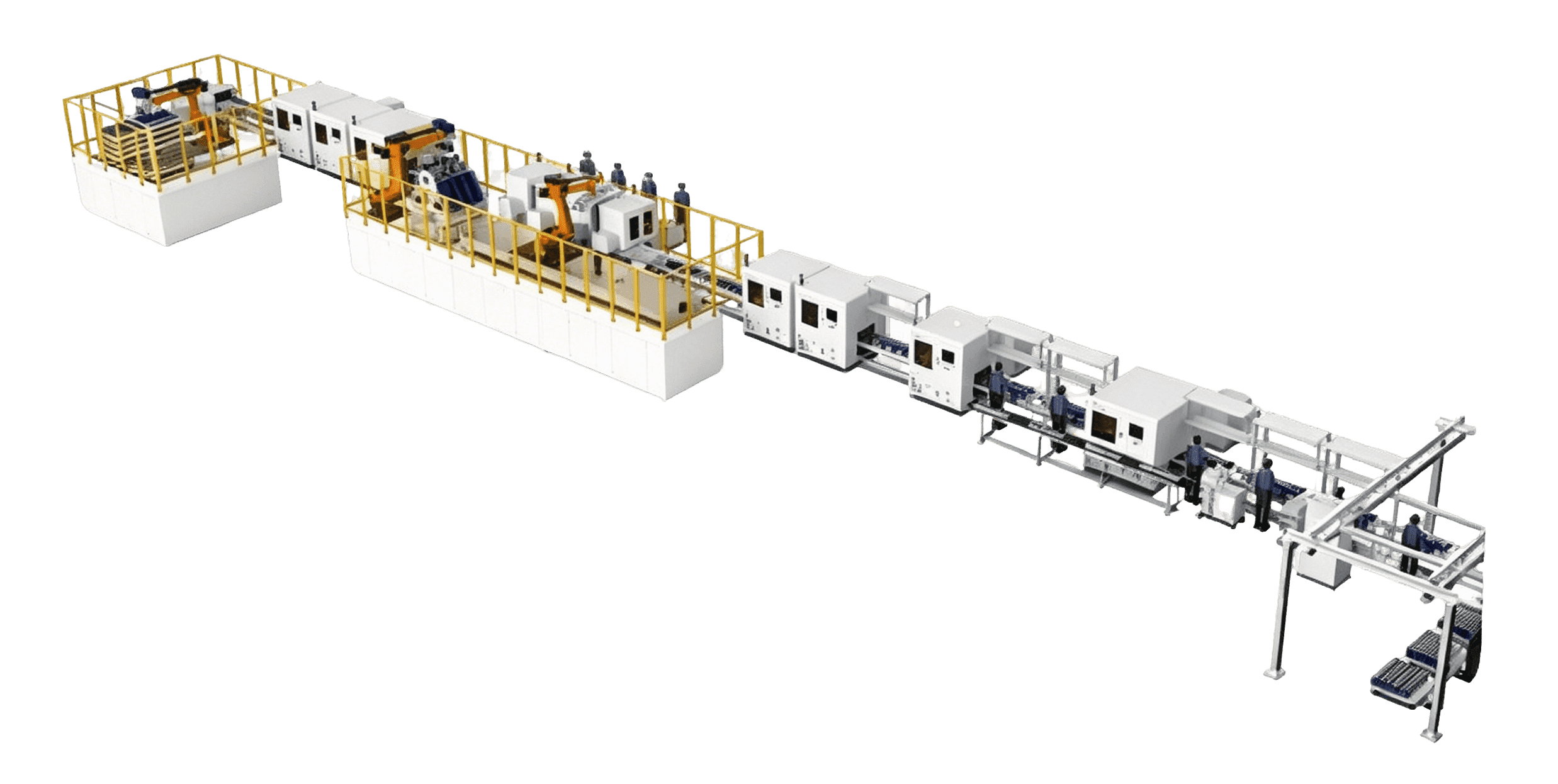
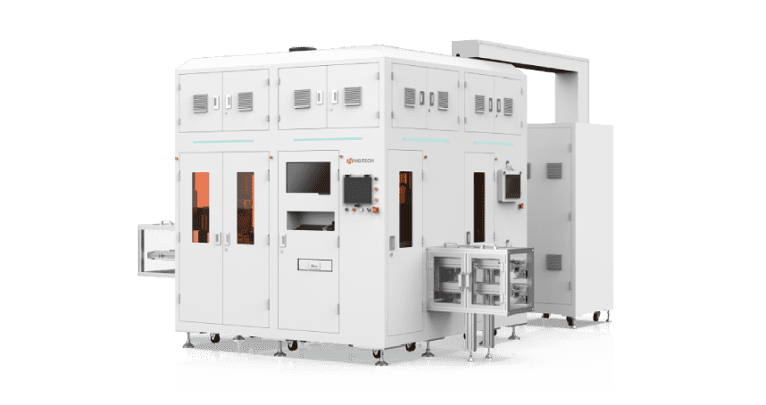
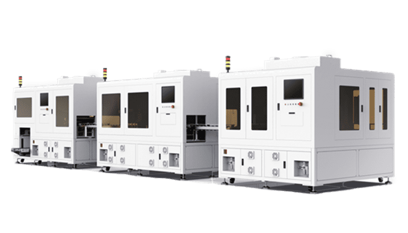
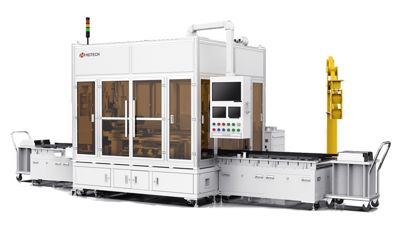
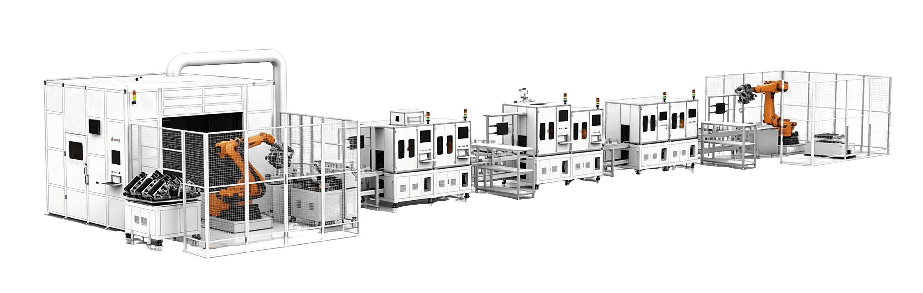
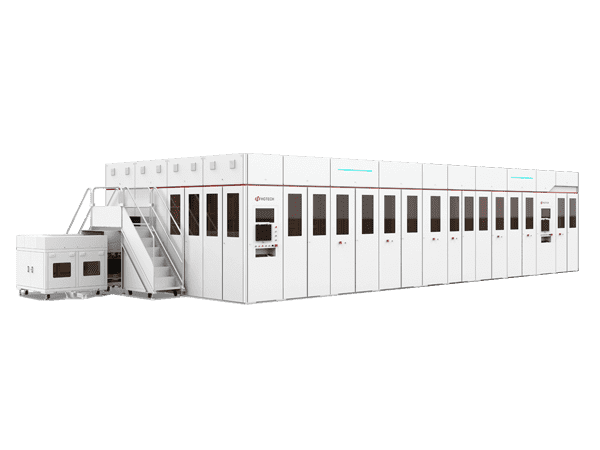
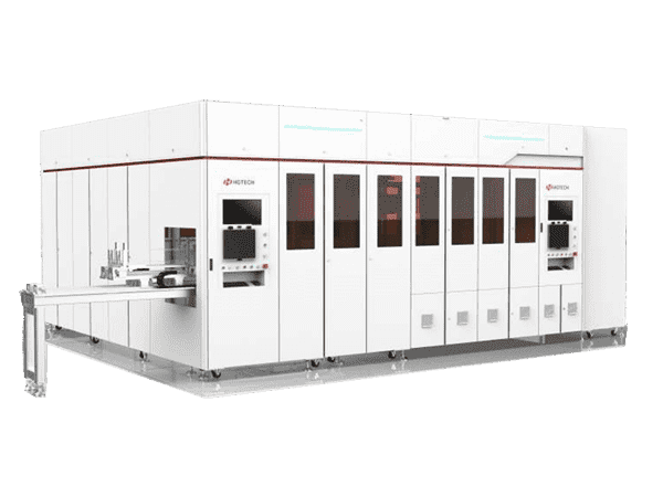
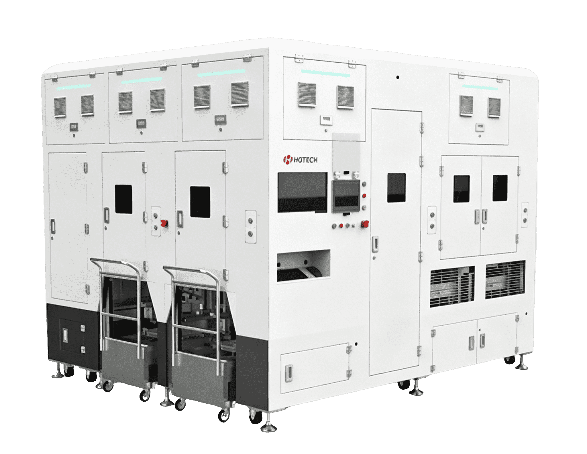
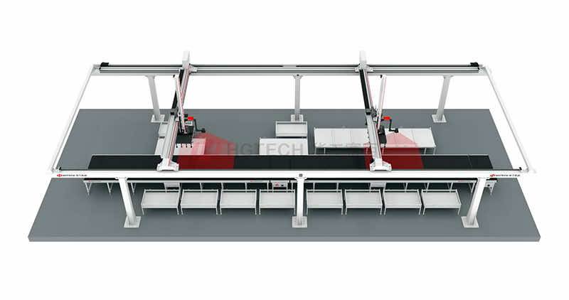
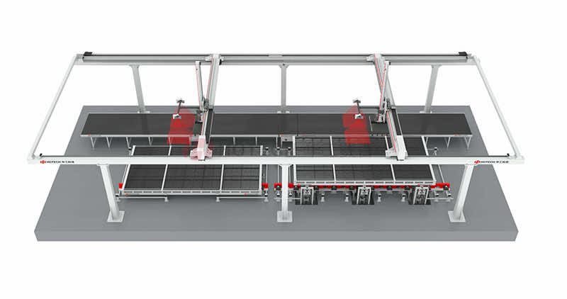
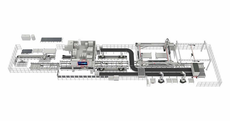
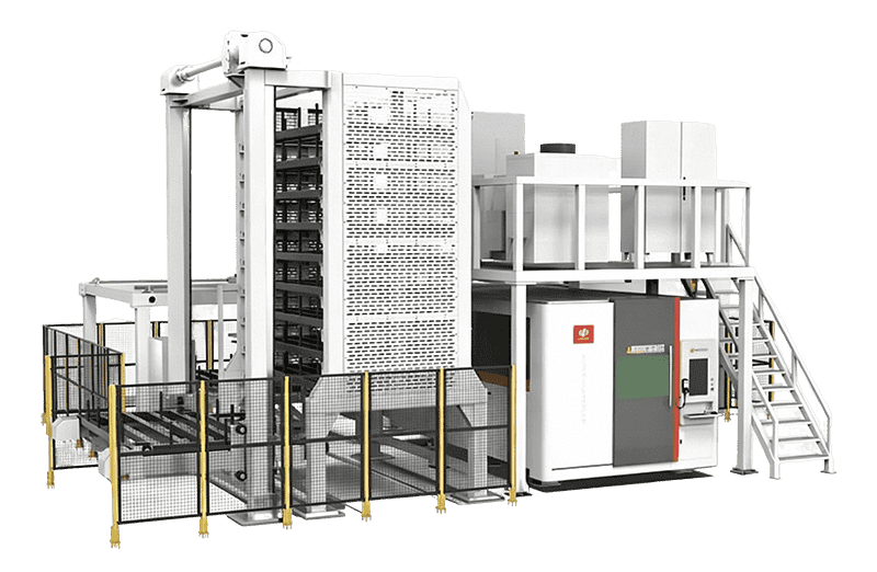
Automotive Laser Manufacturing


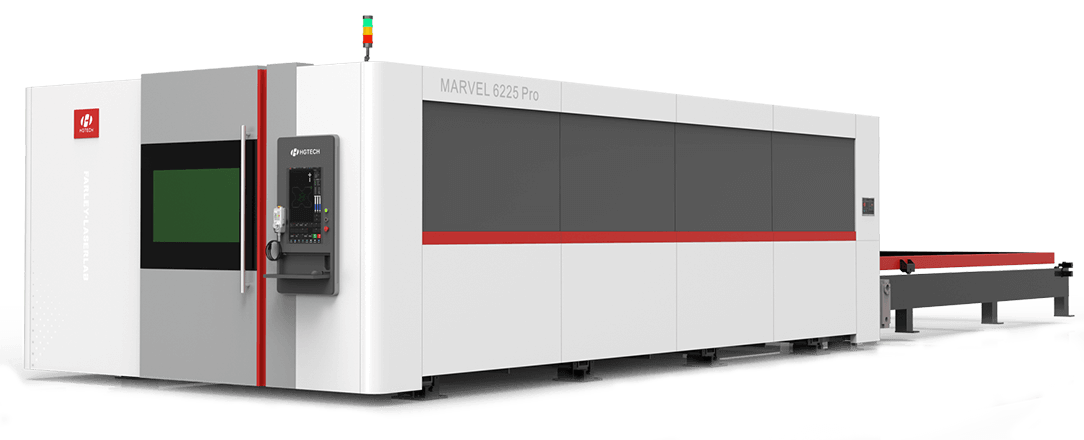
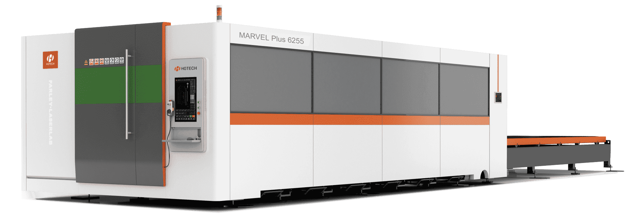
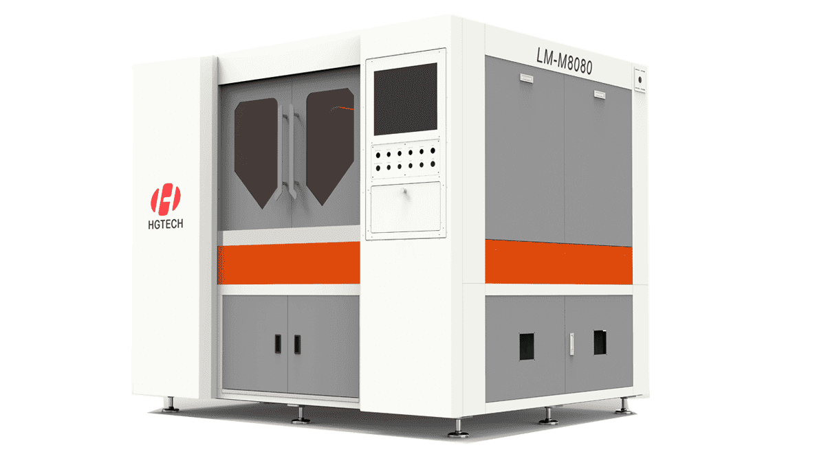
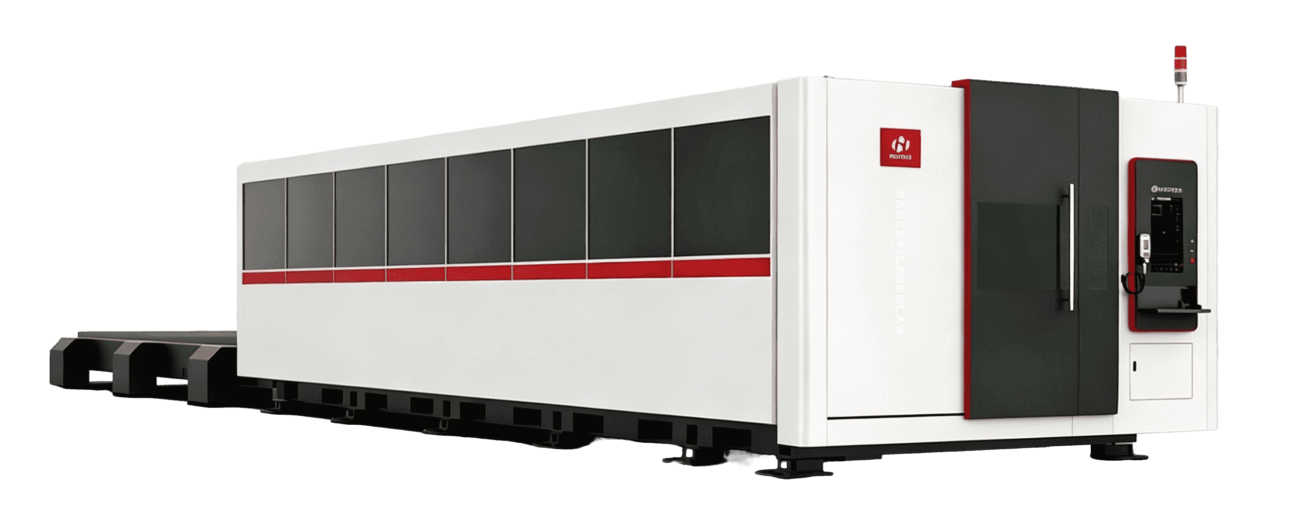
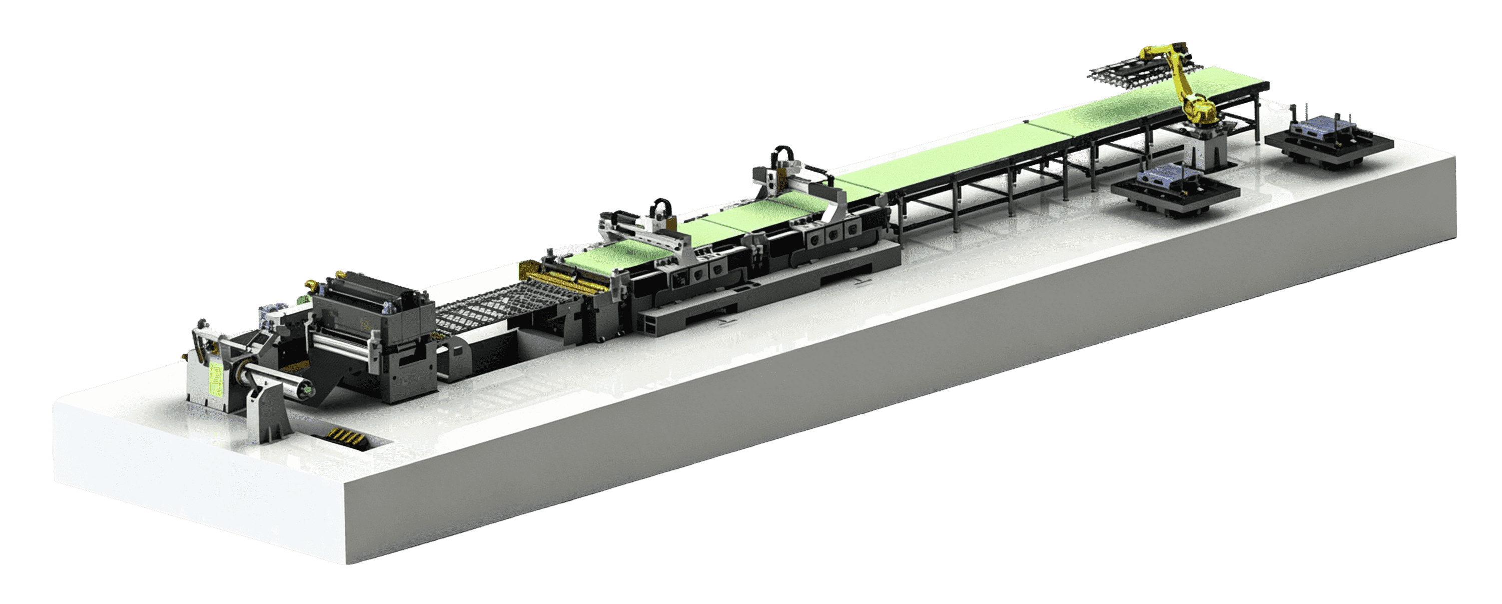
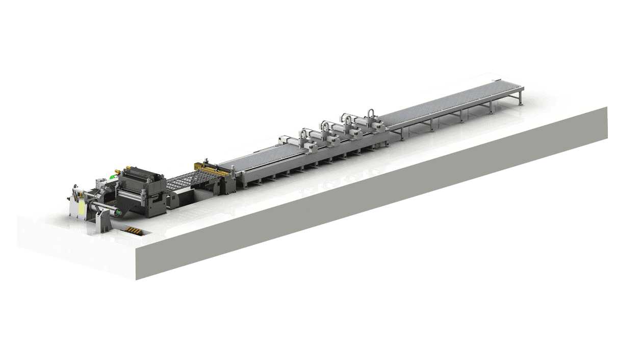
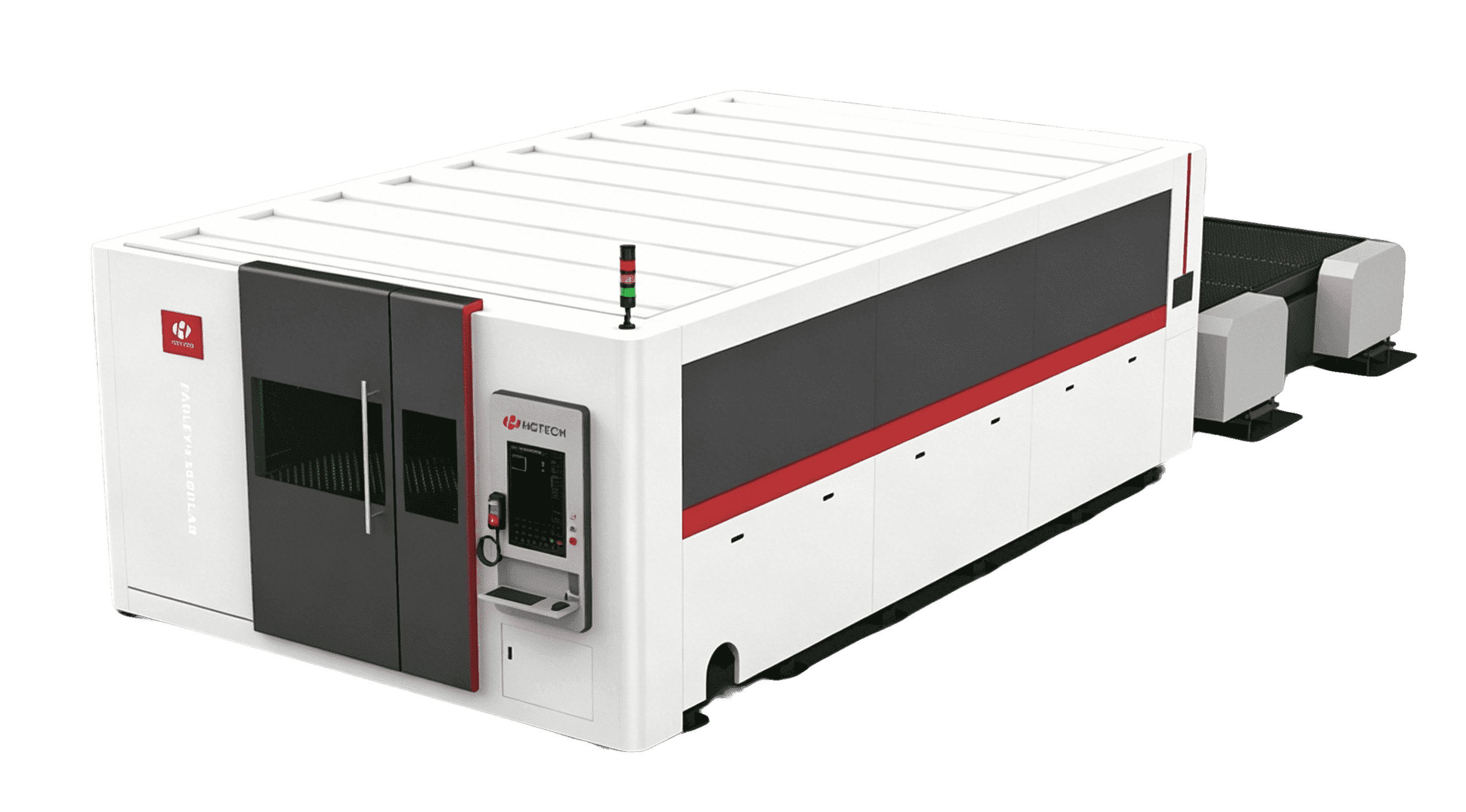
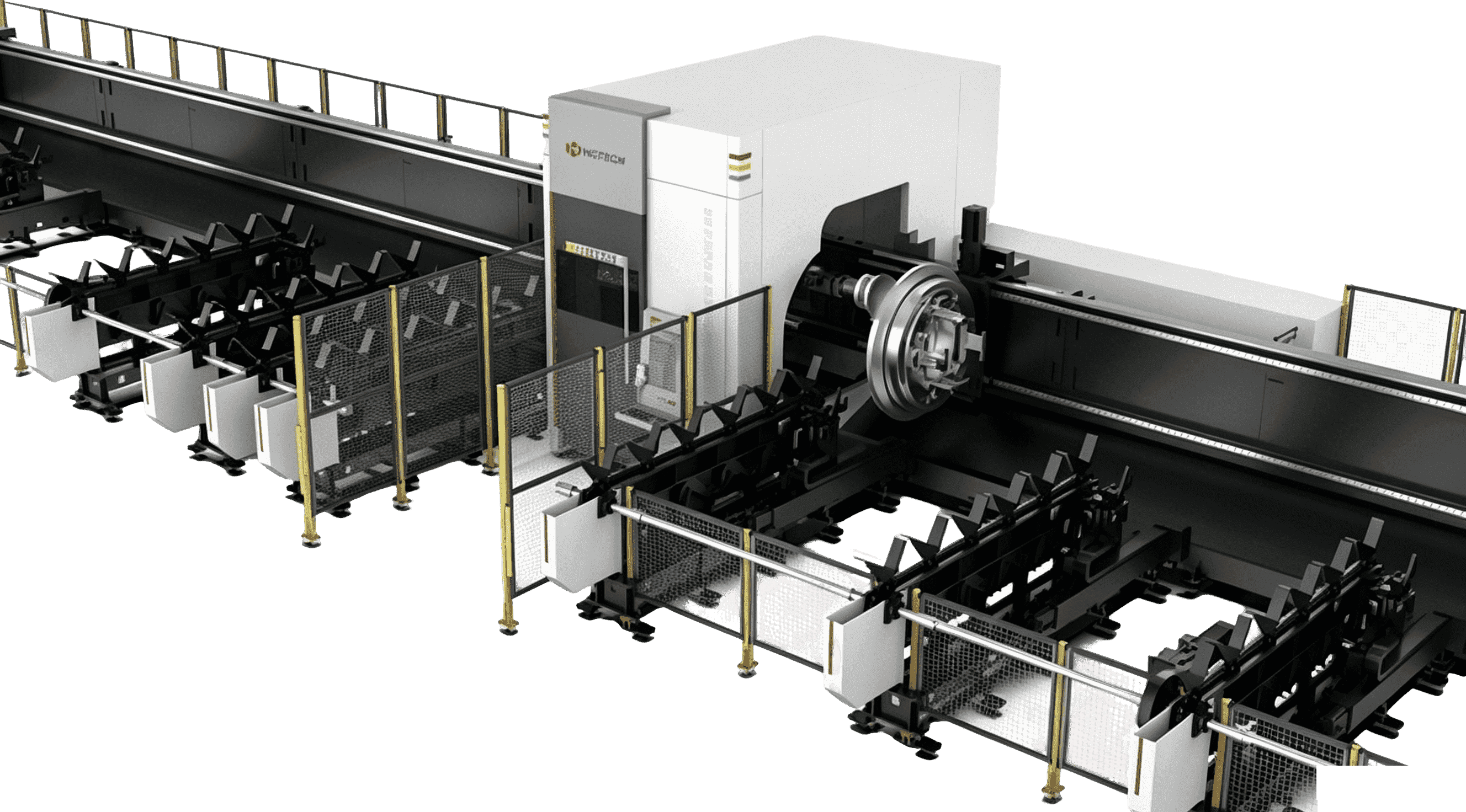
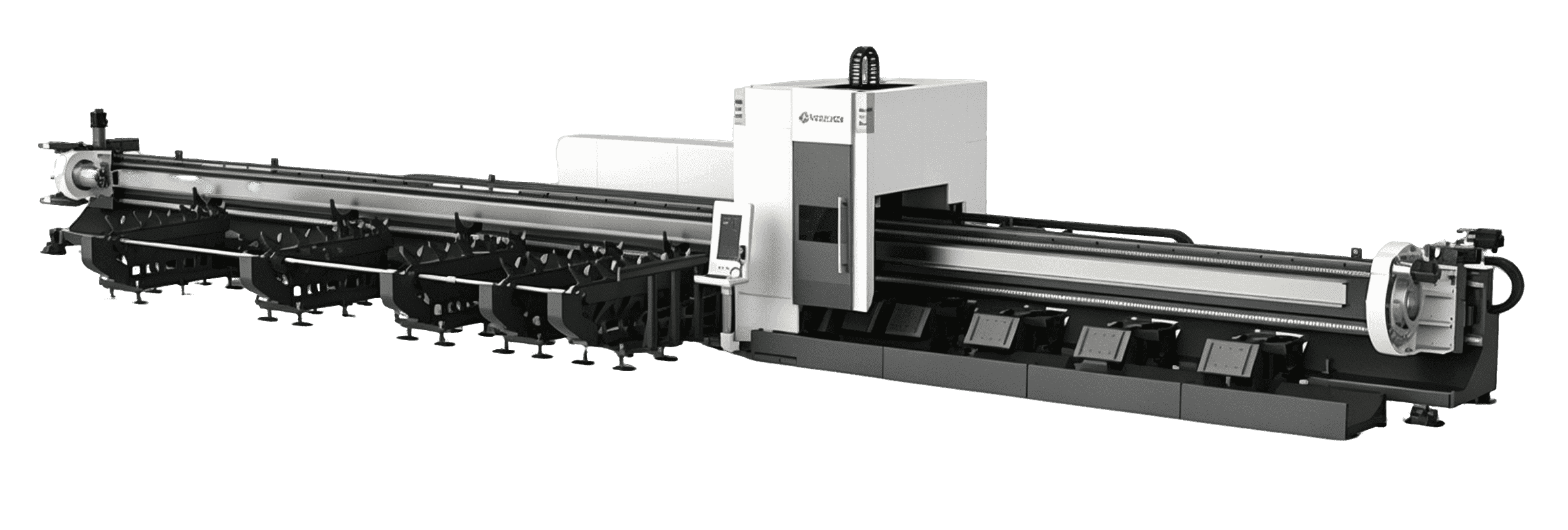
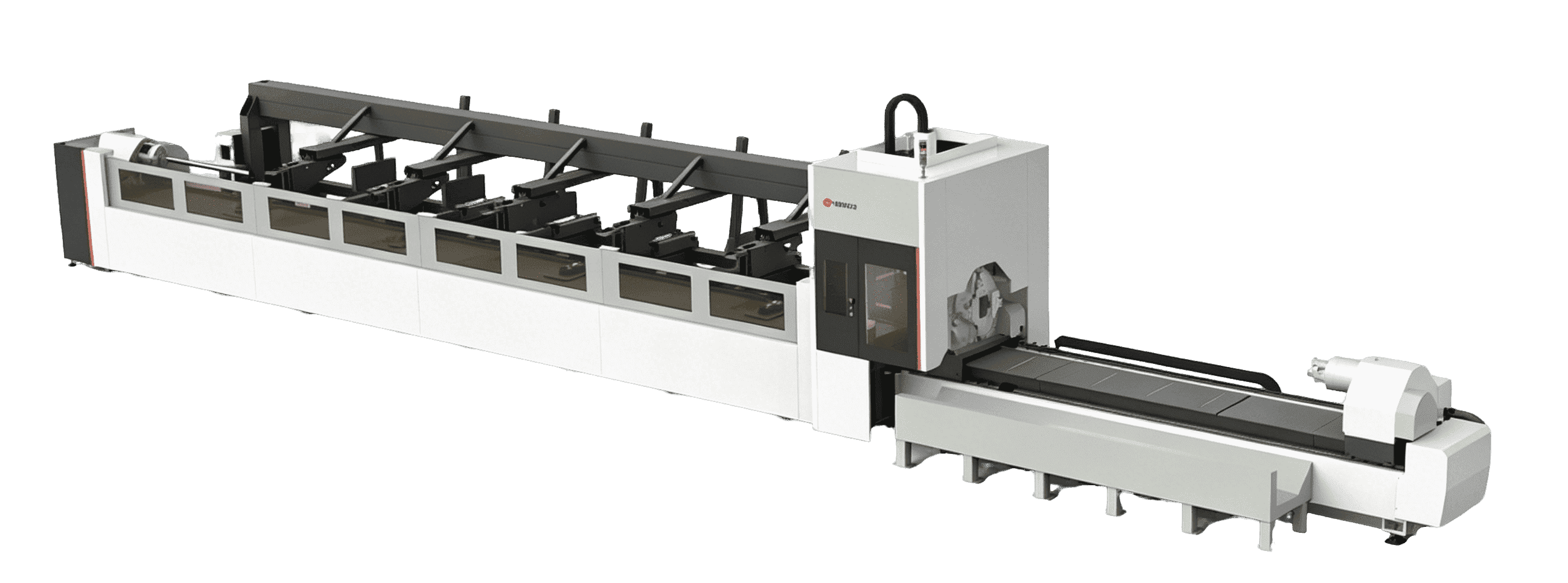
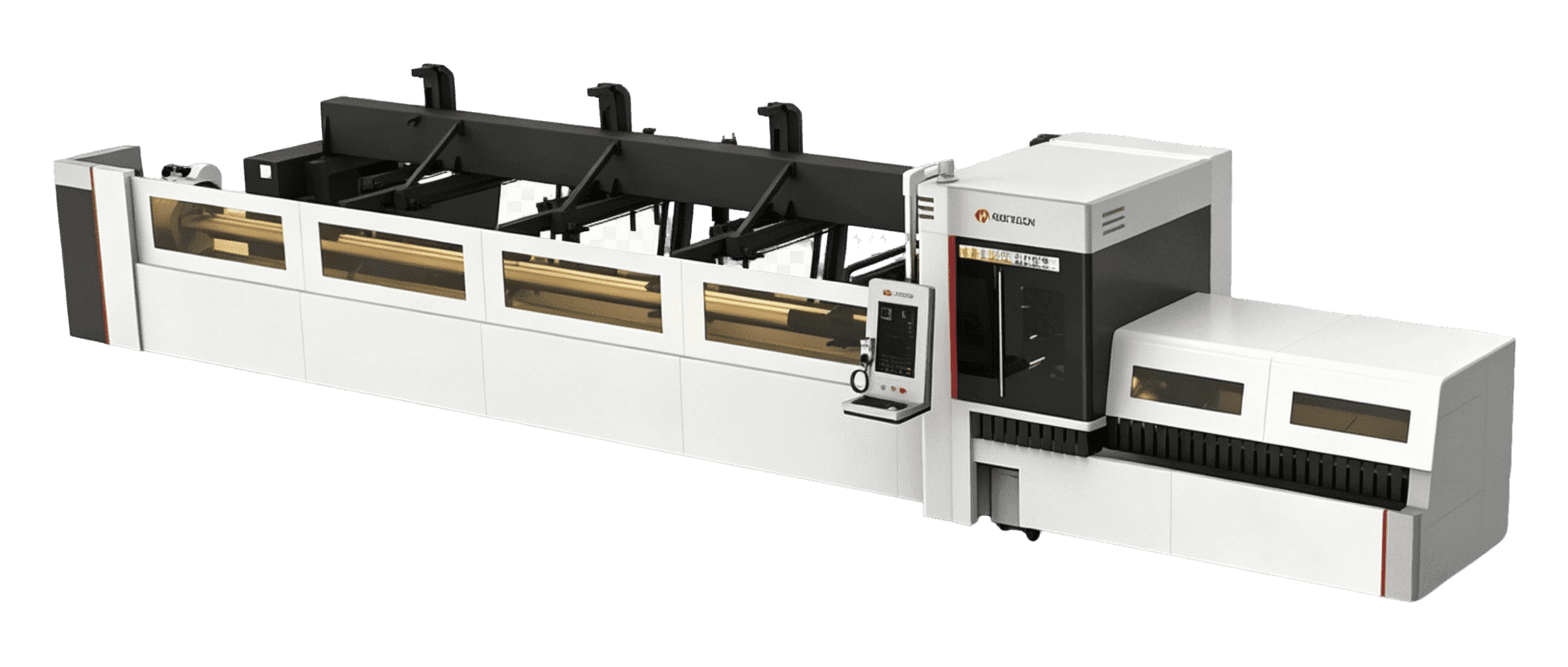
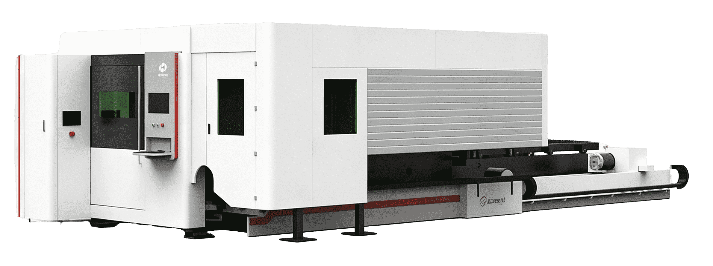
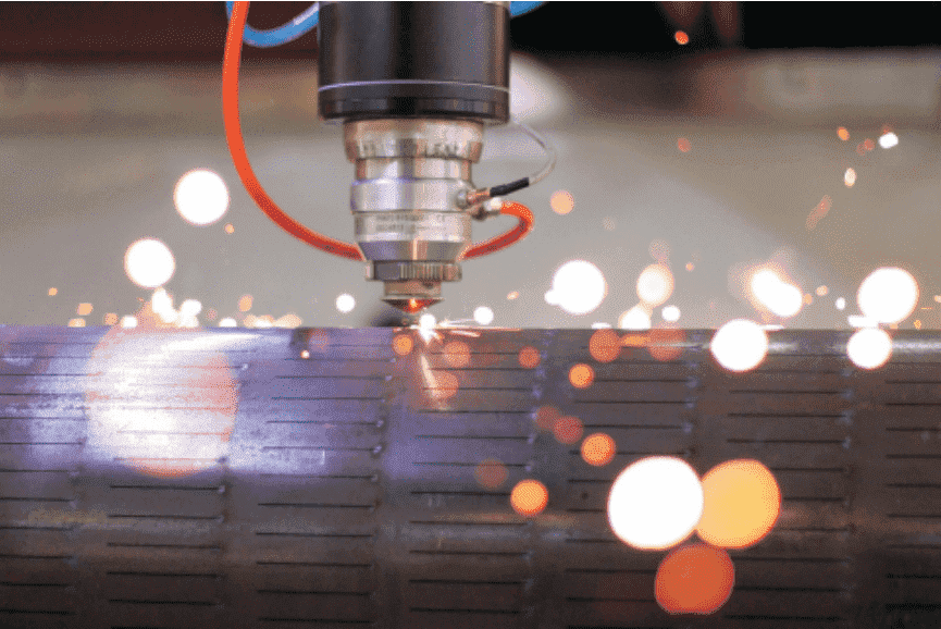
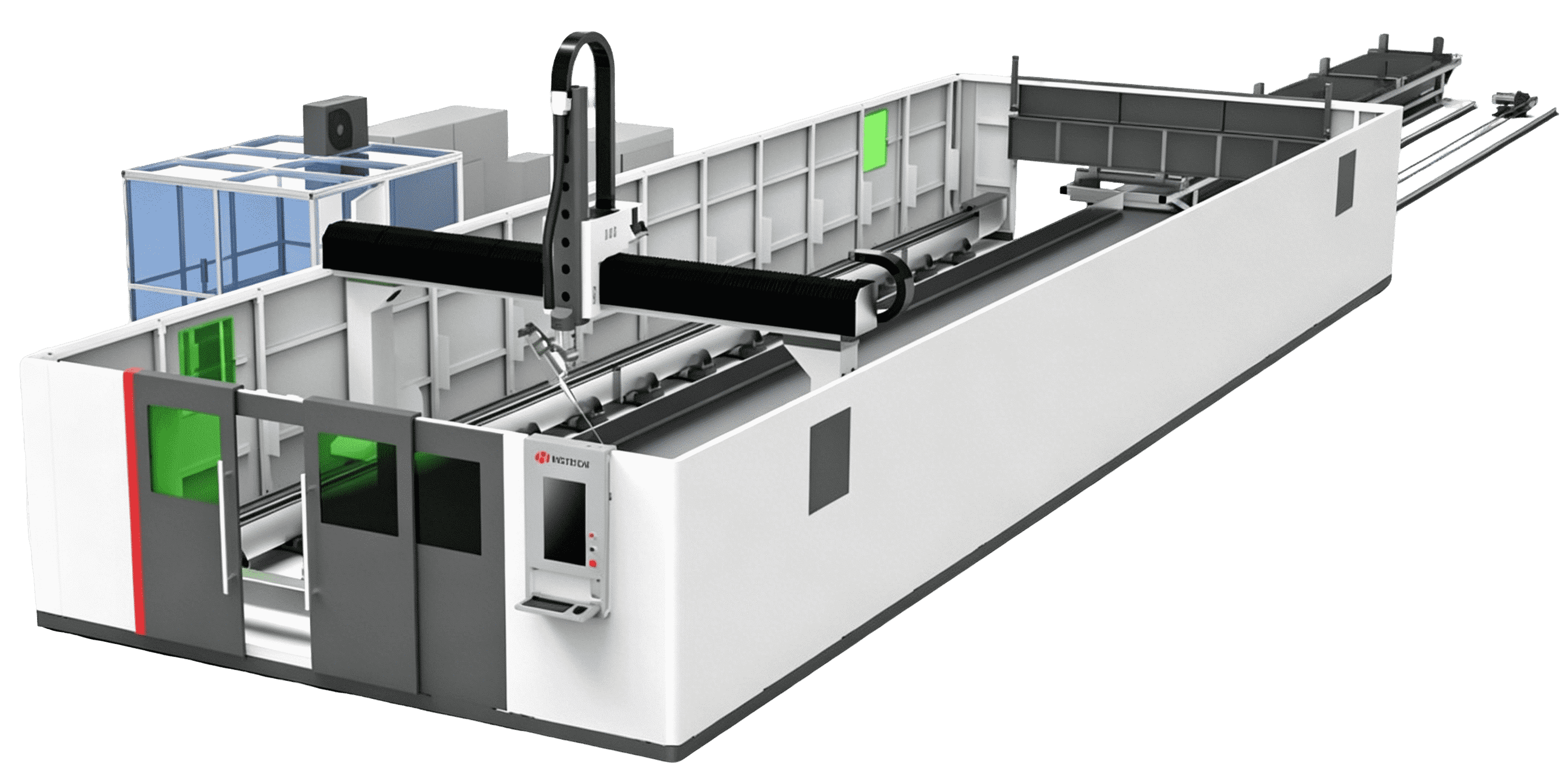
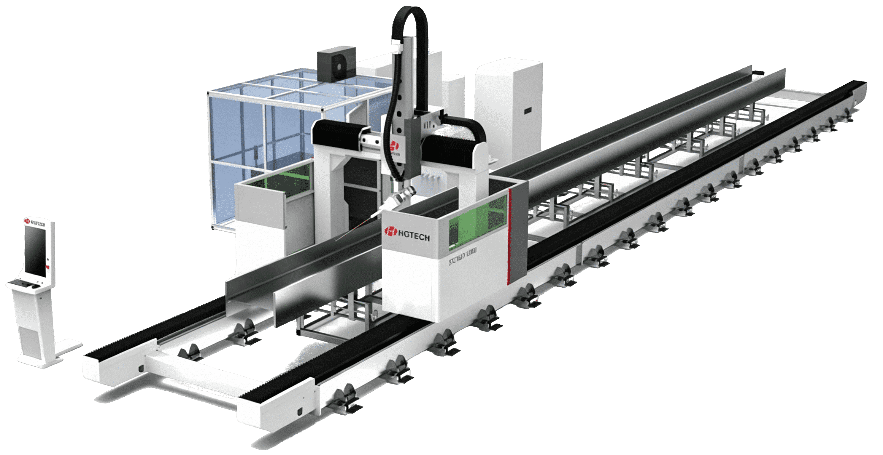
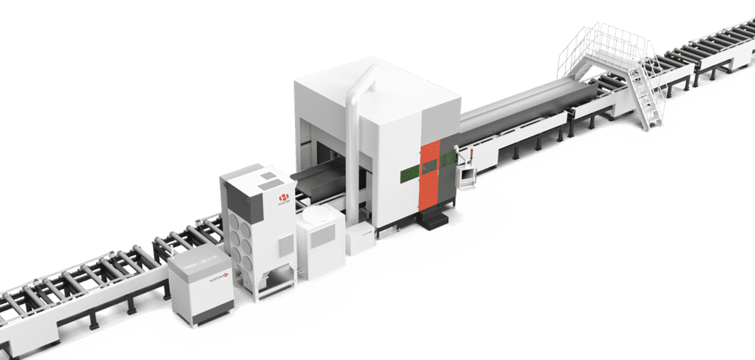
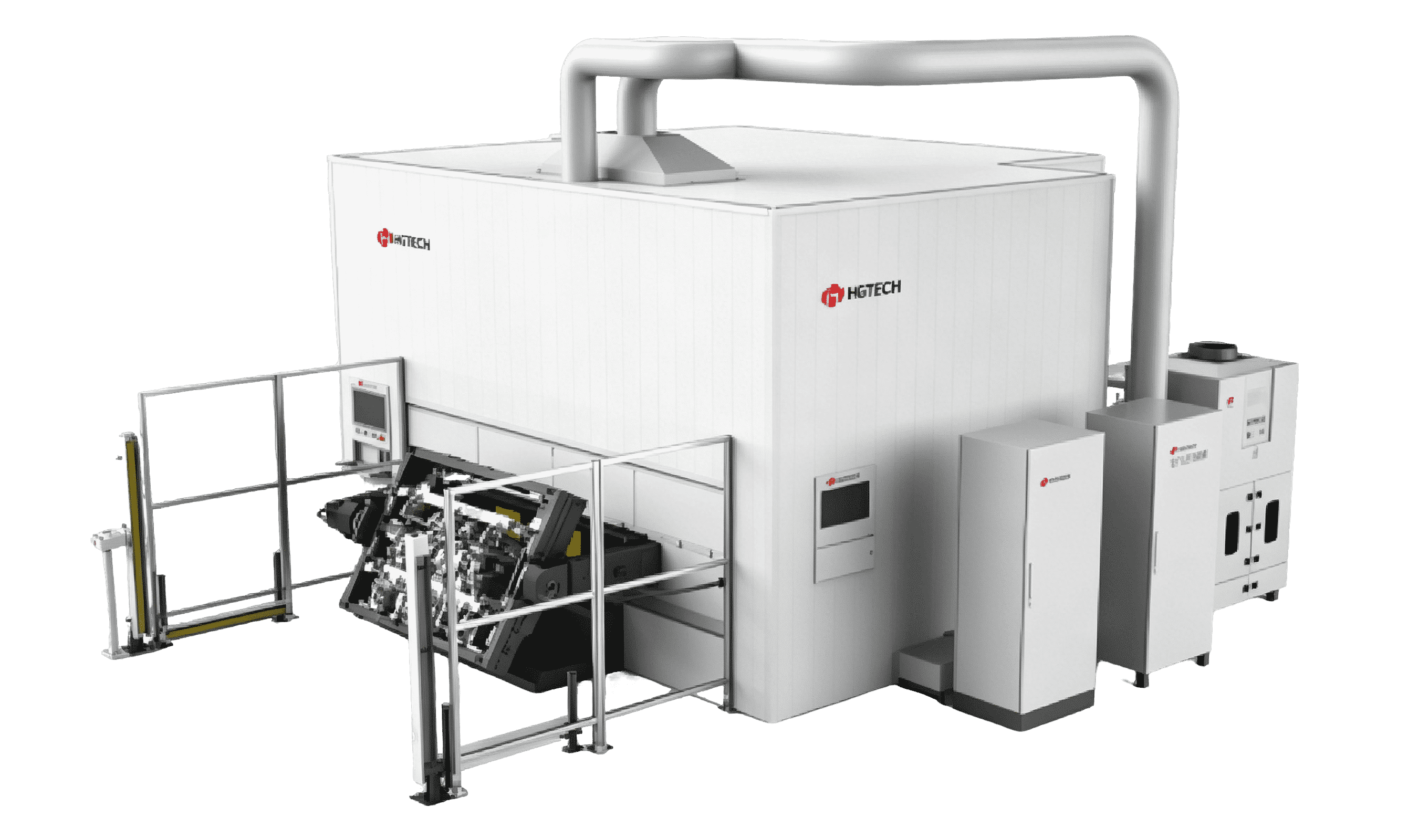
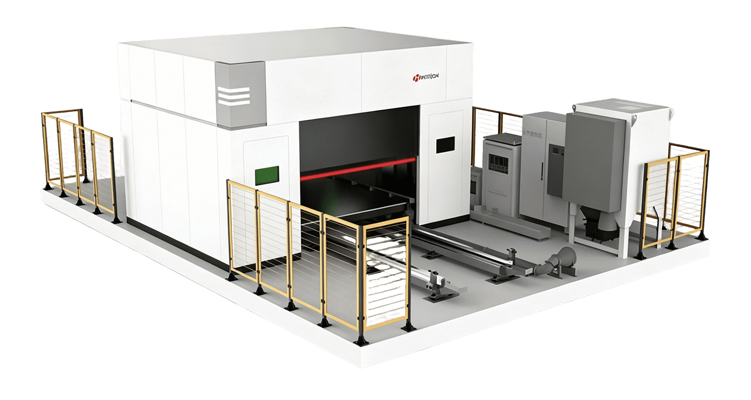
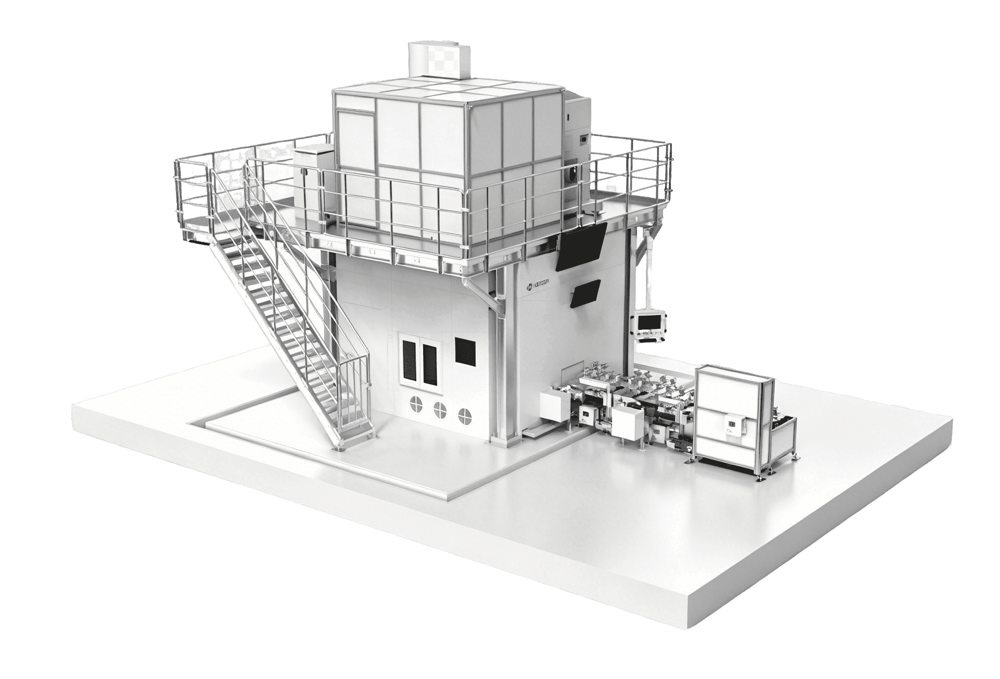
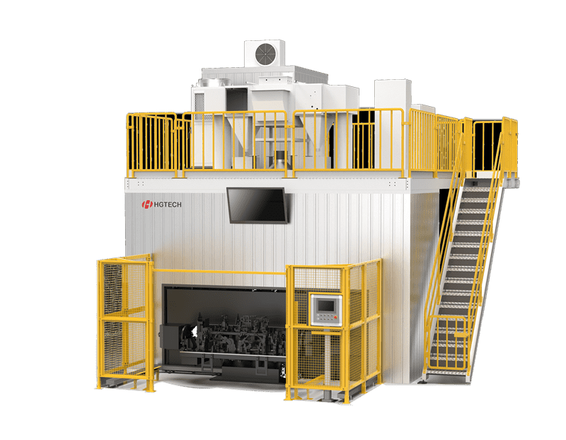
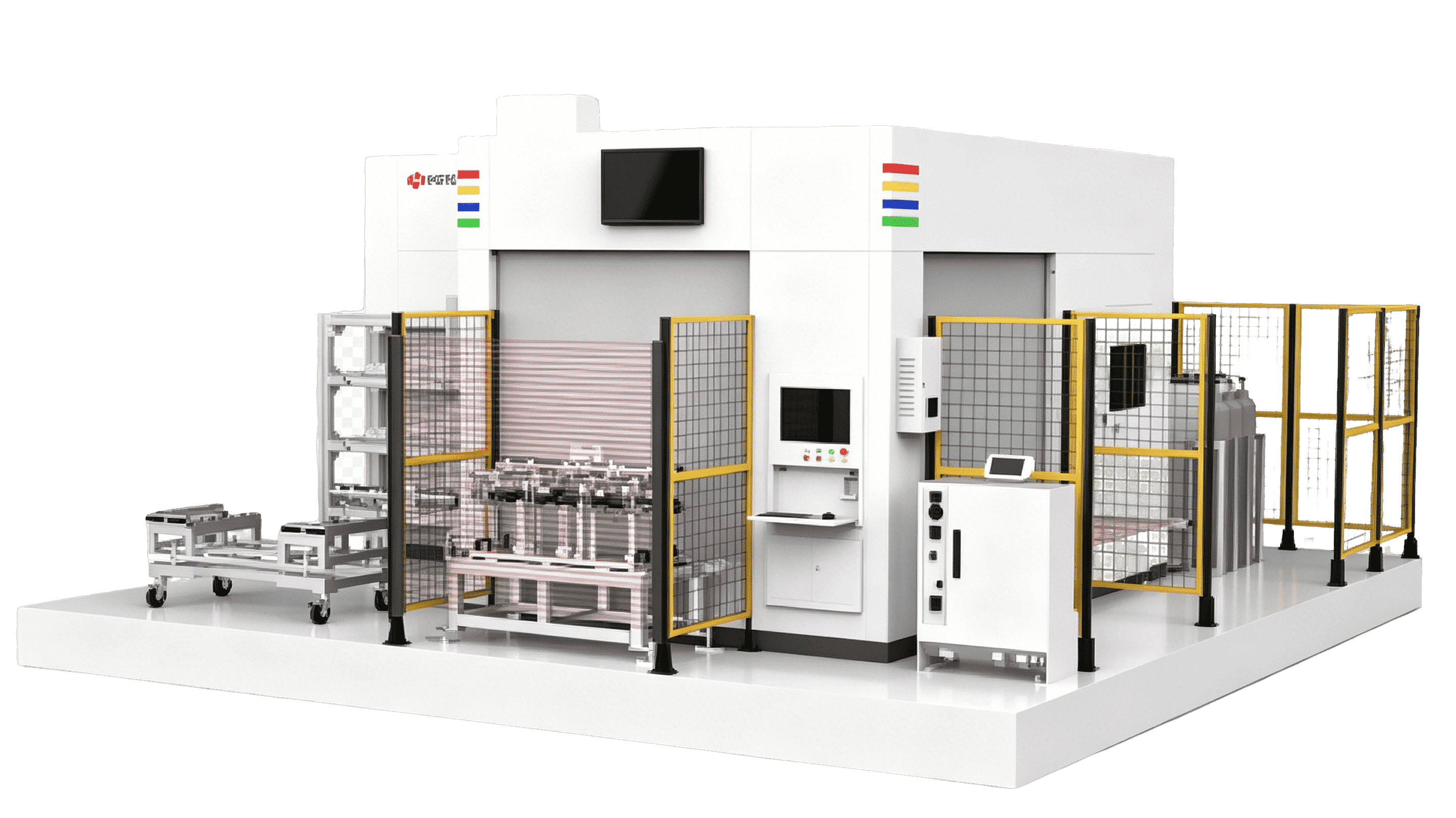
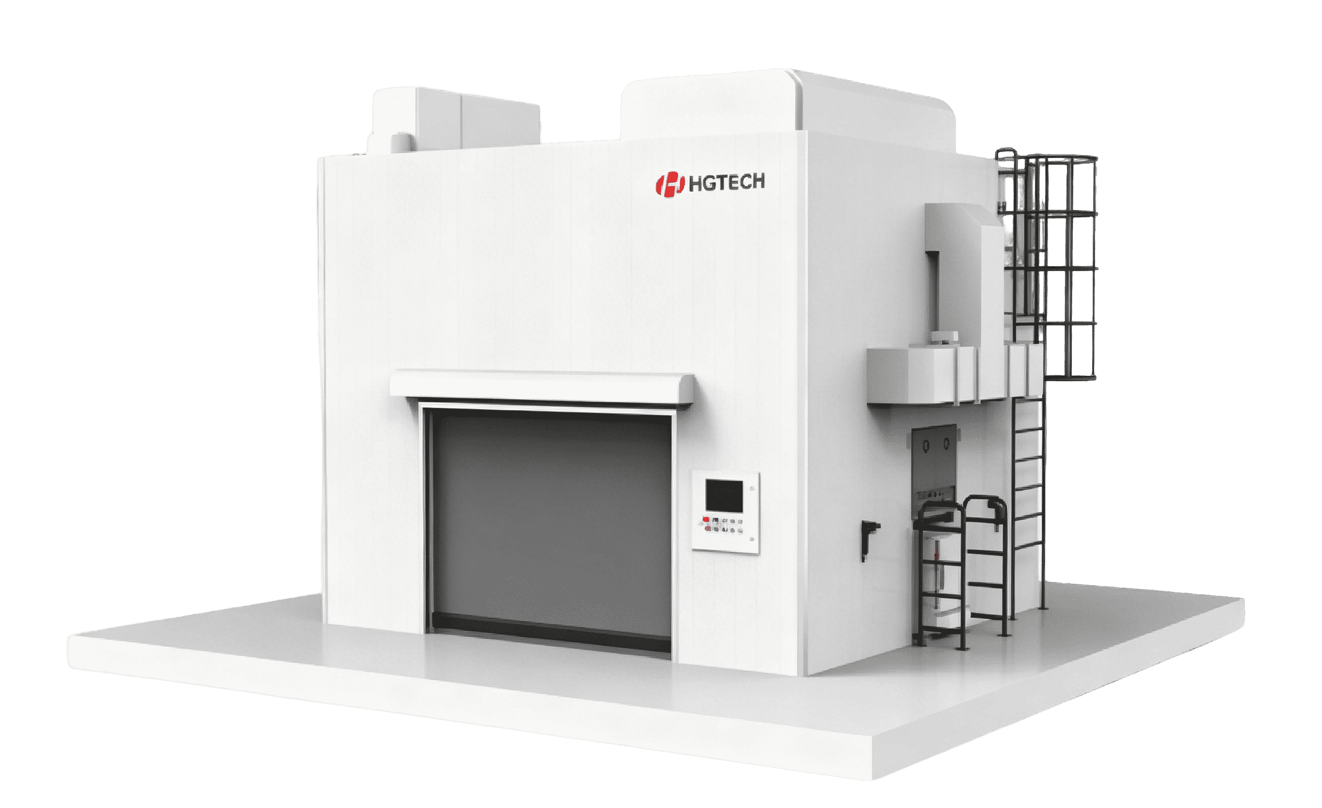
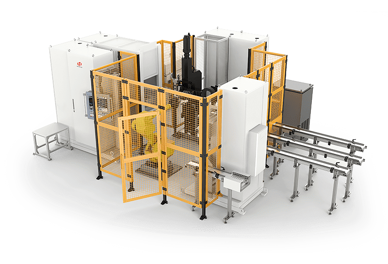
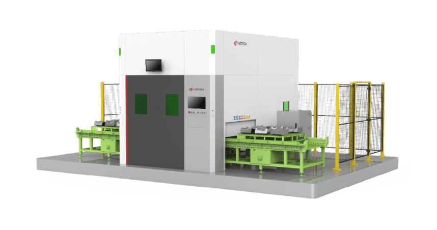
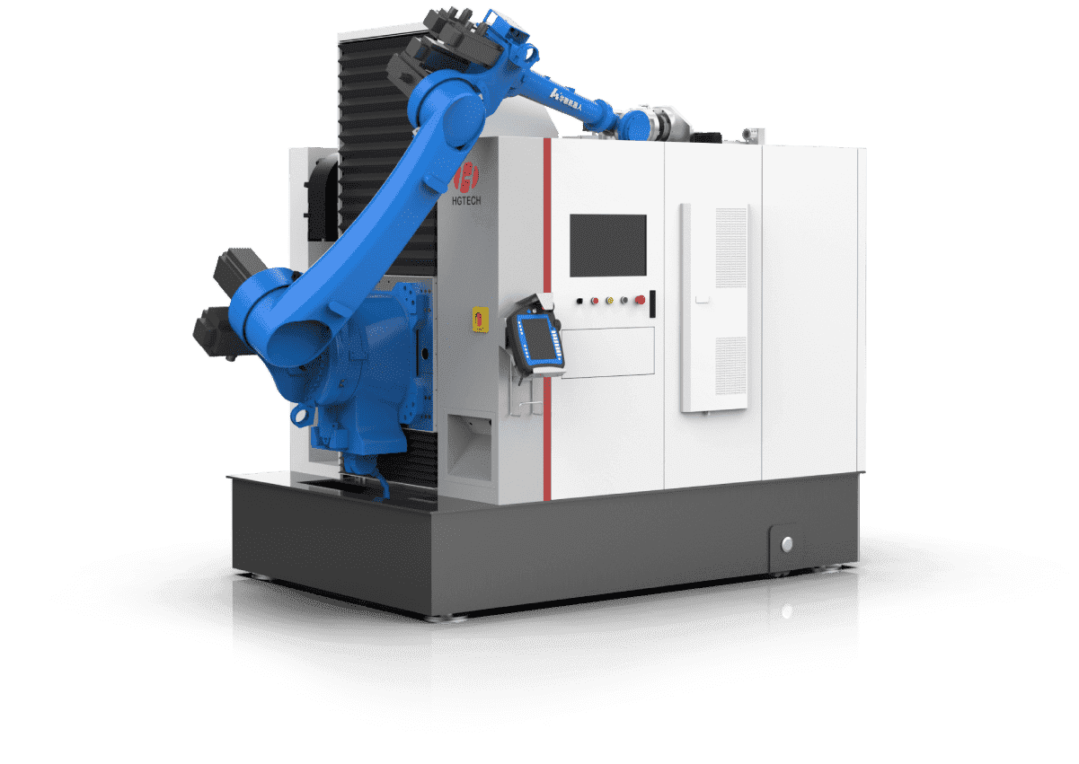
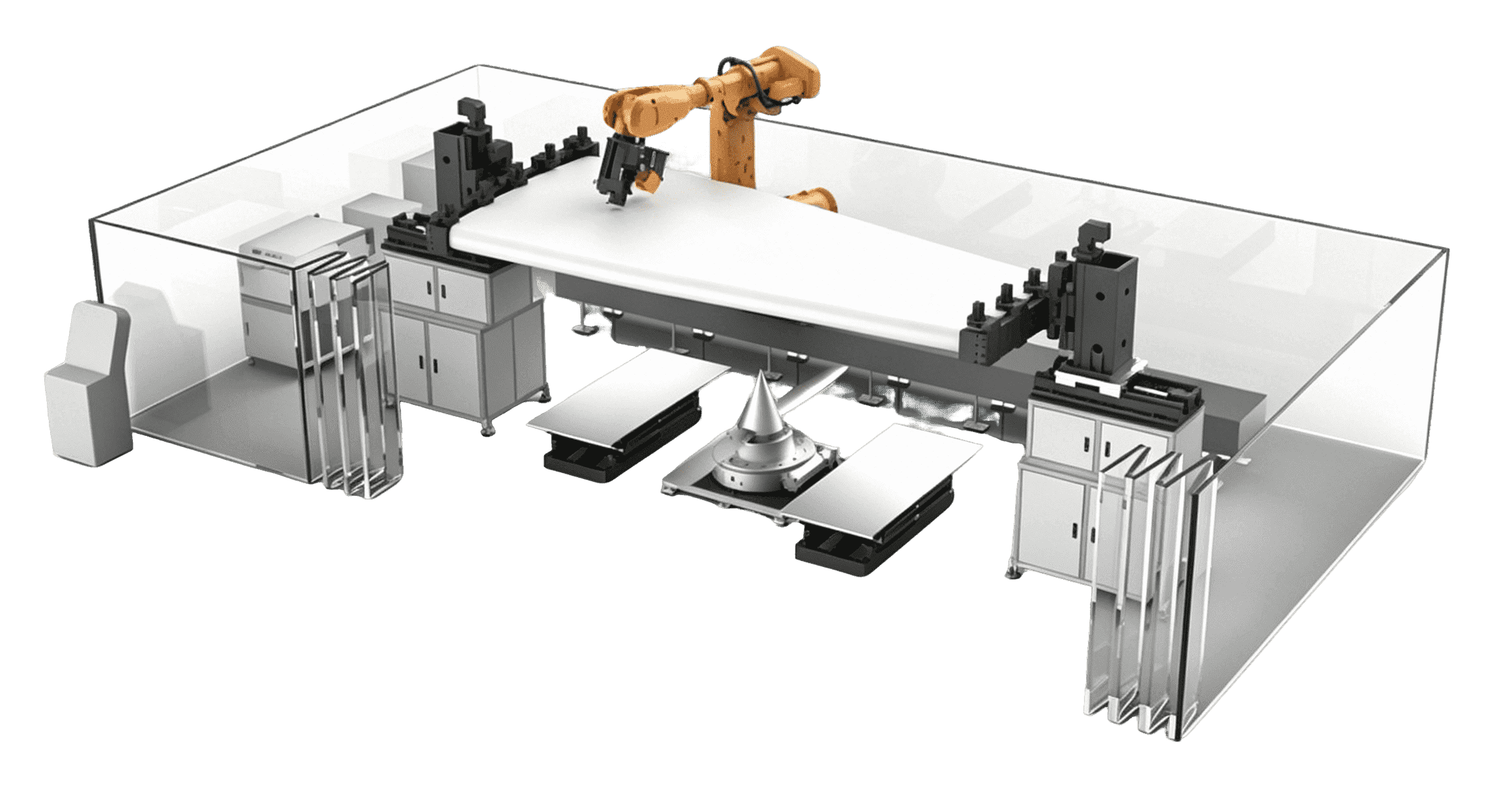
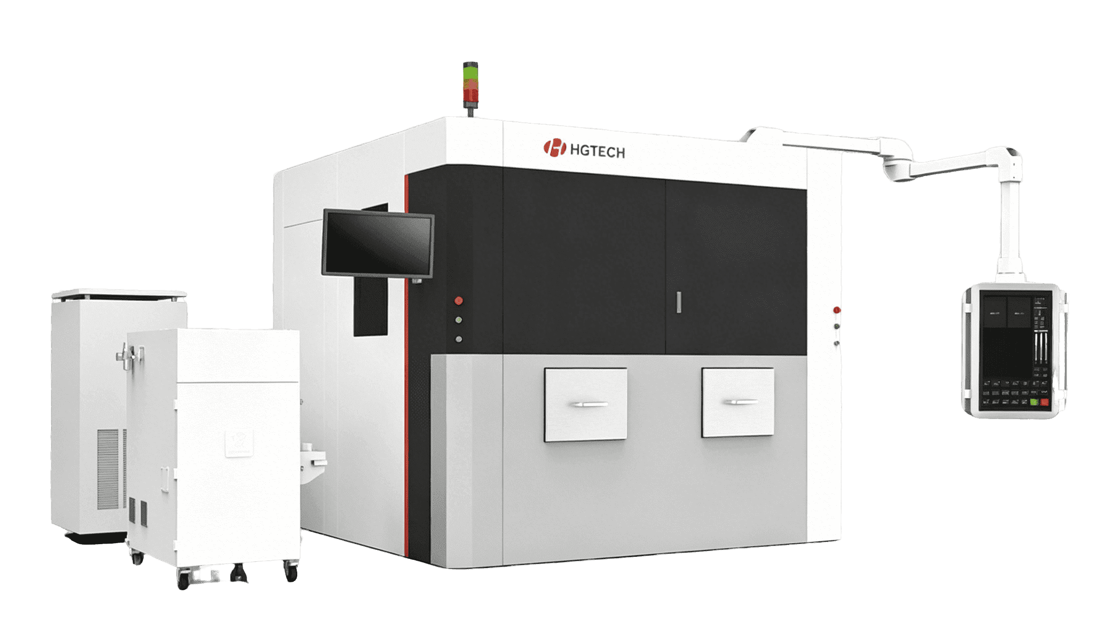

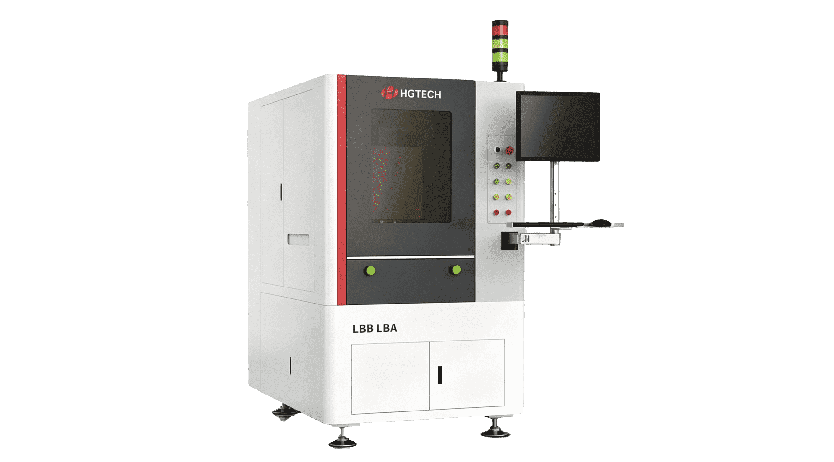
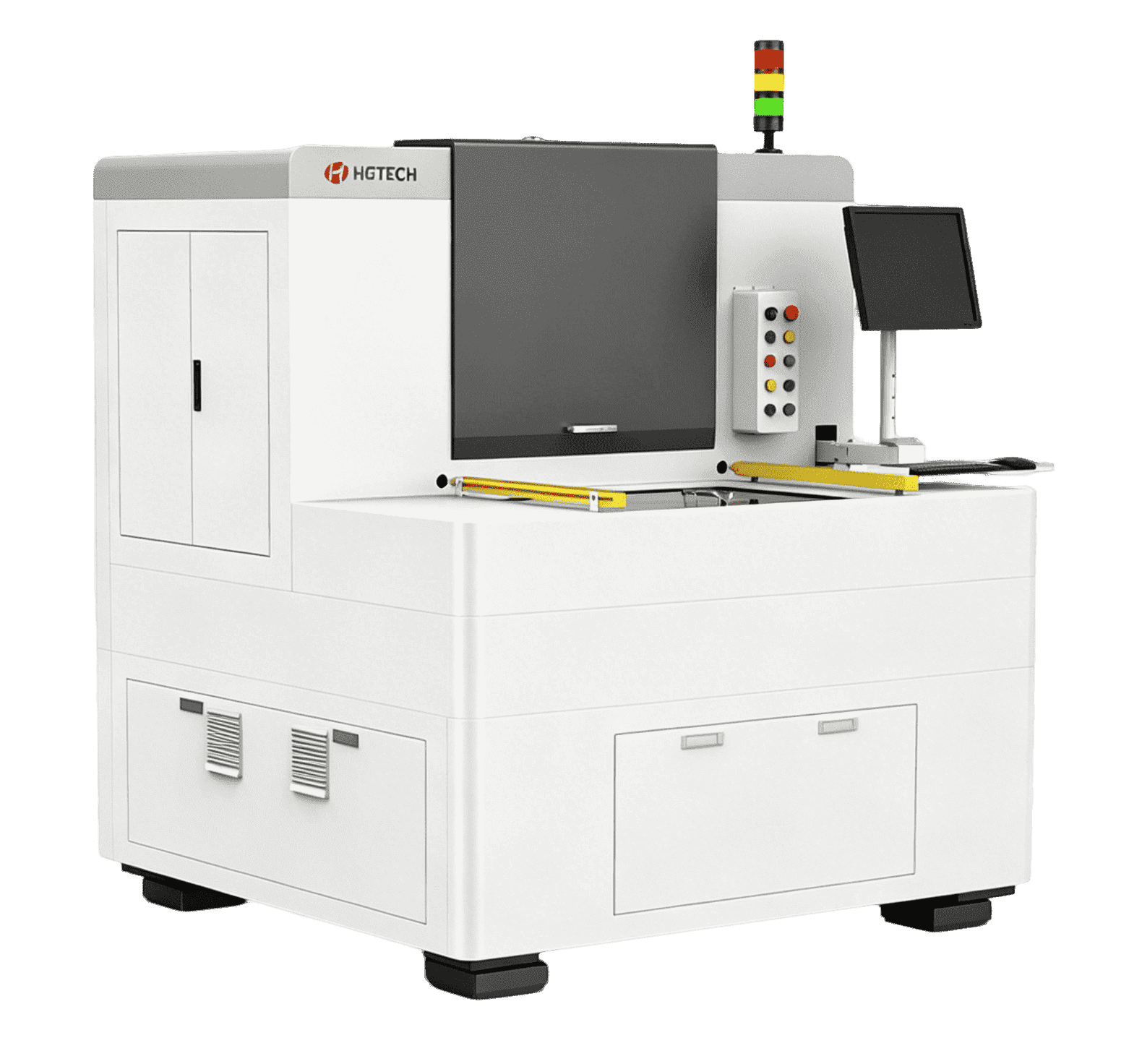
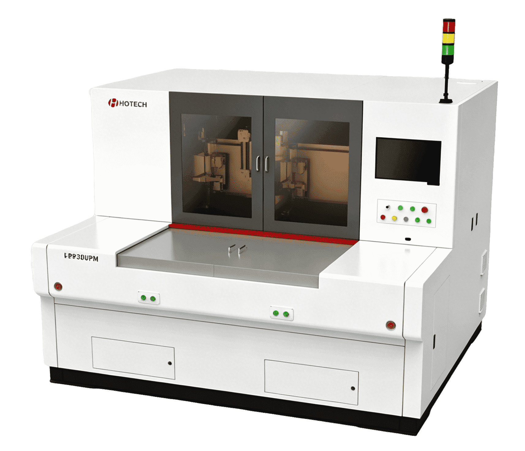
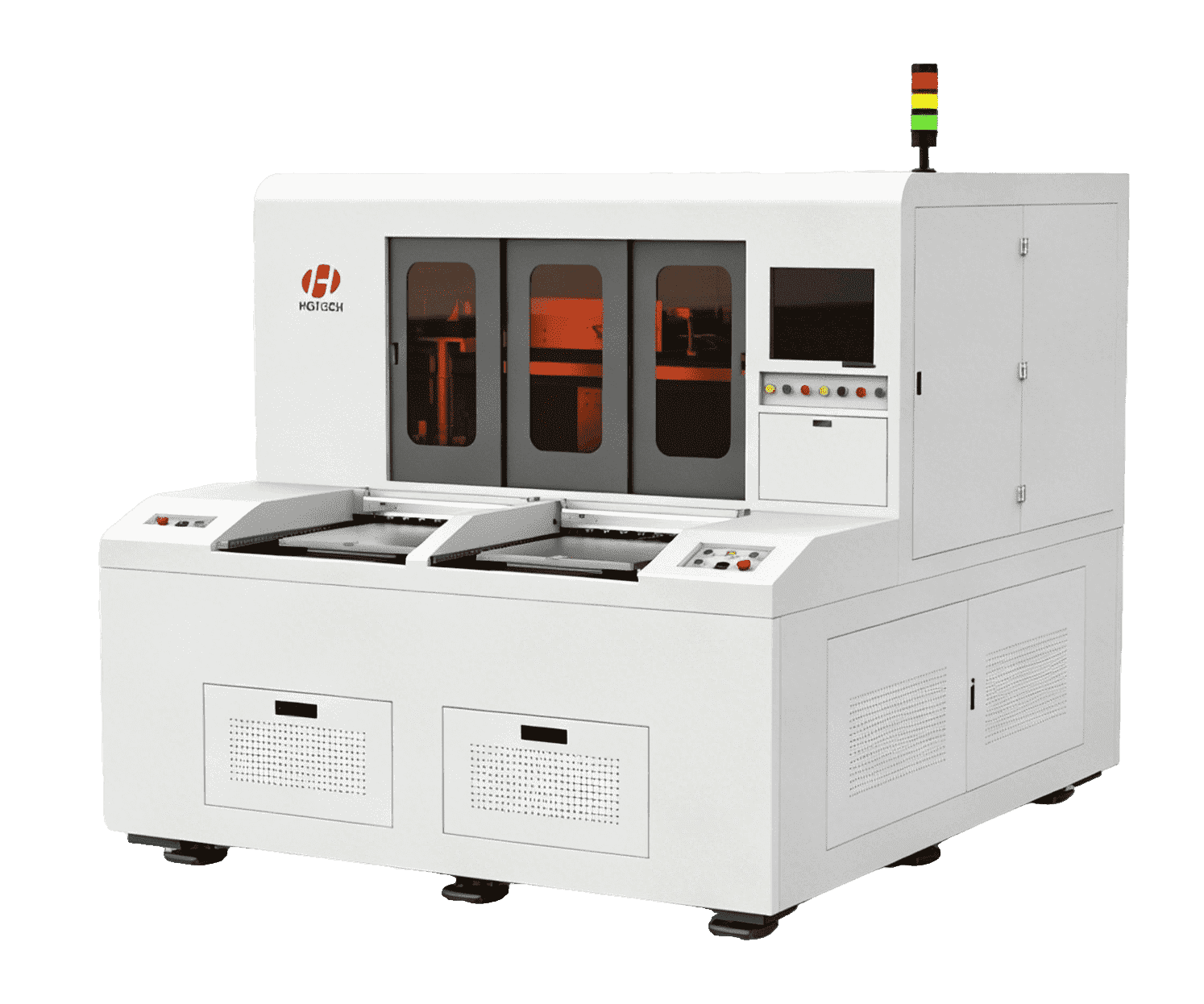
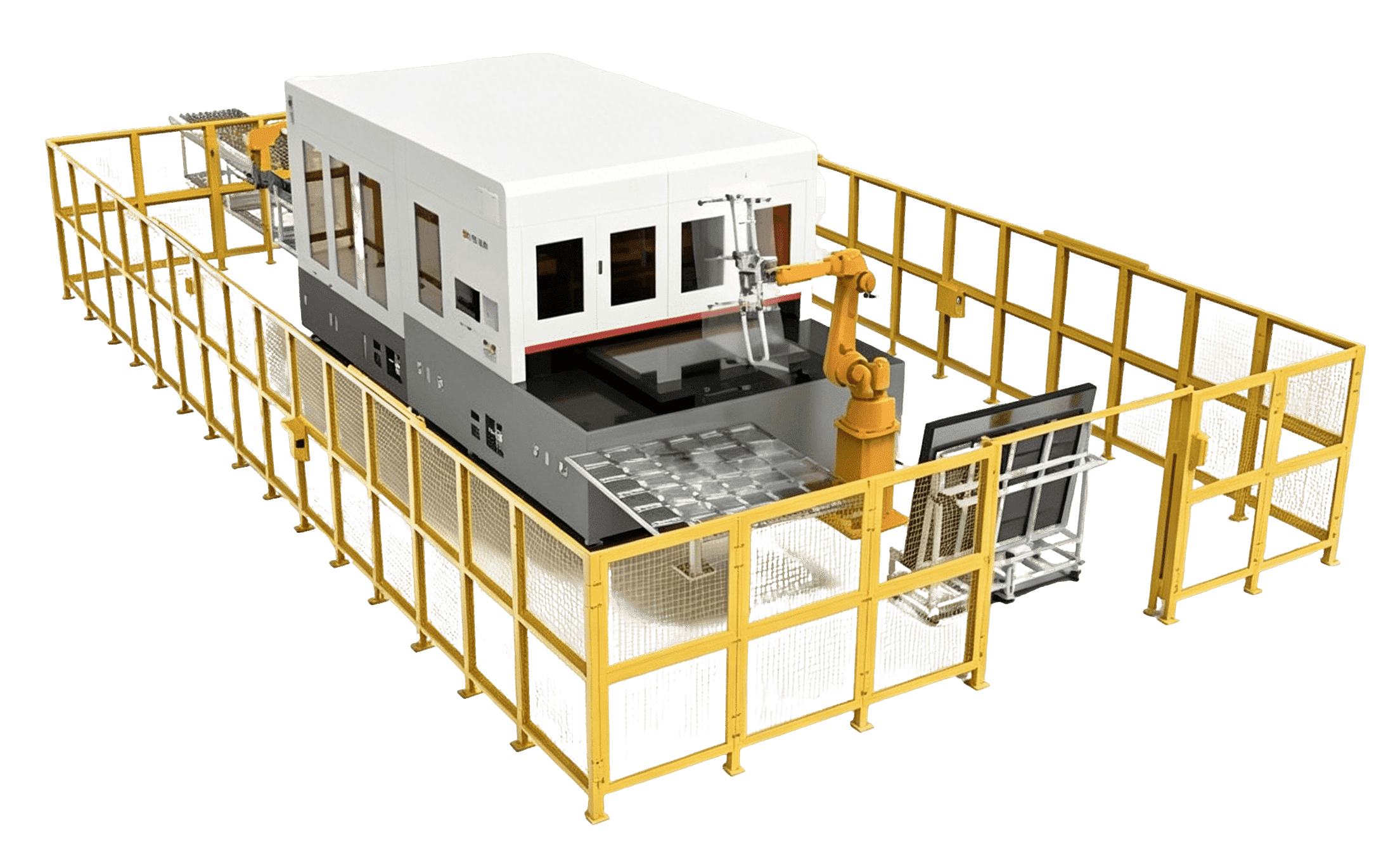
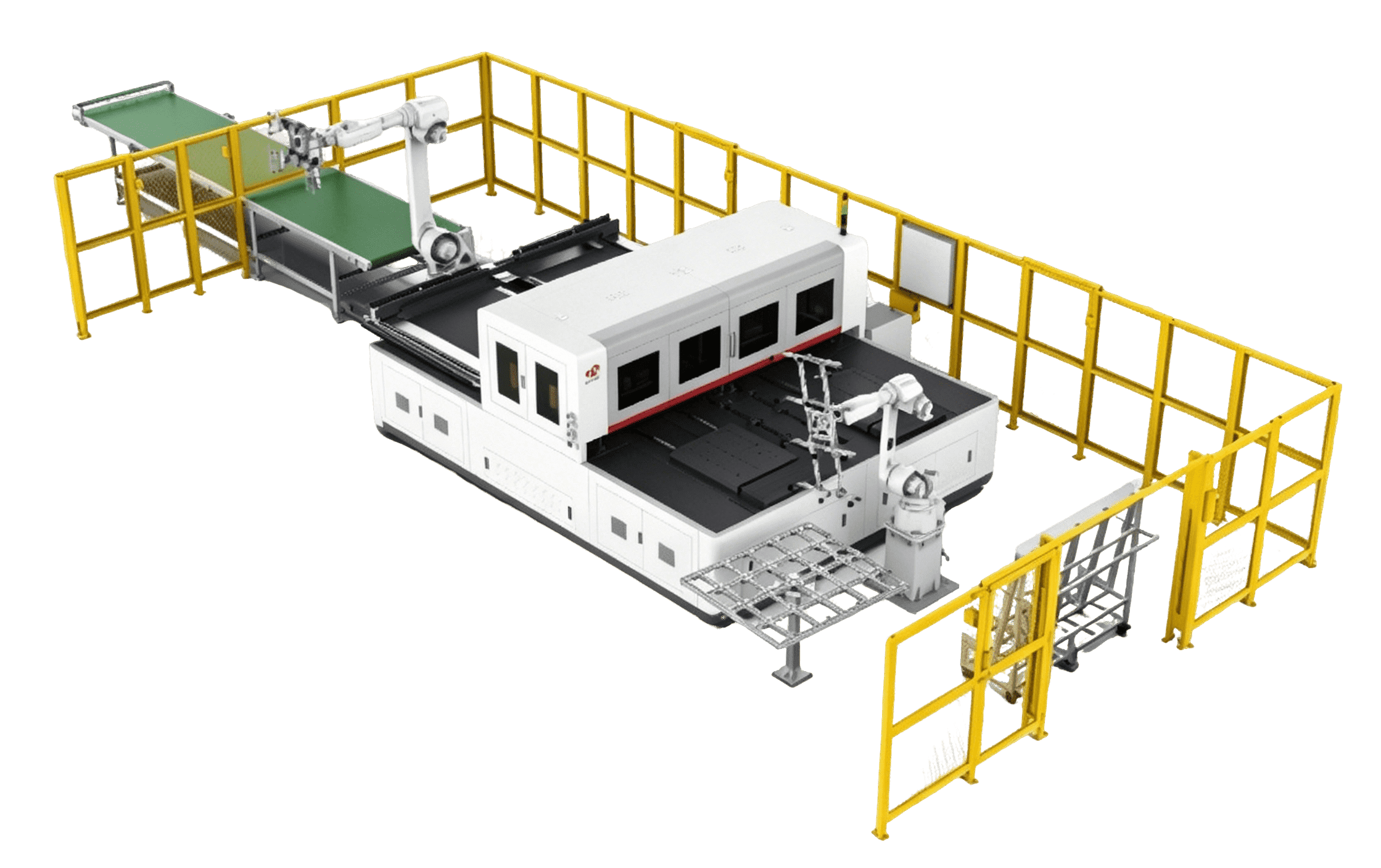
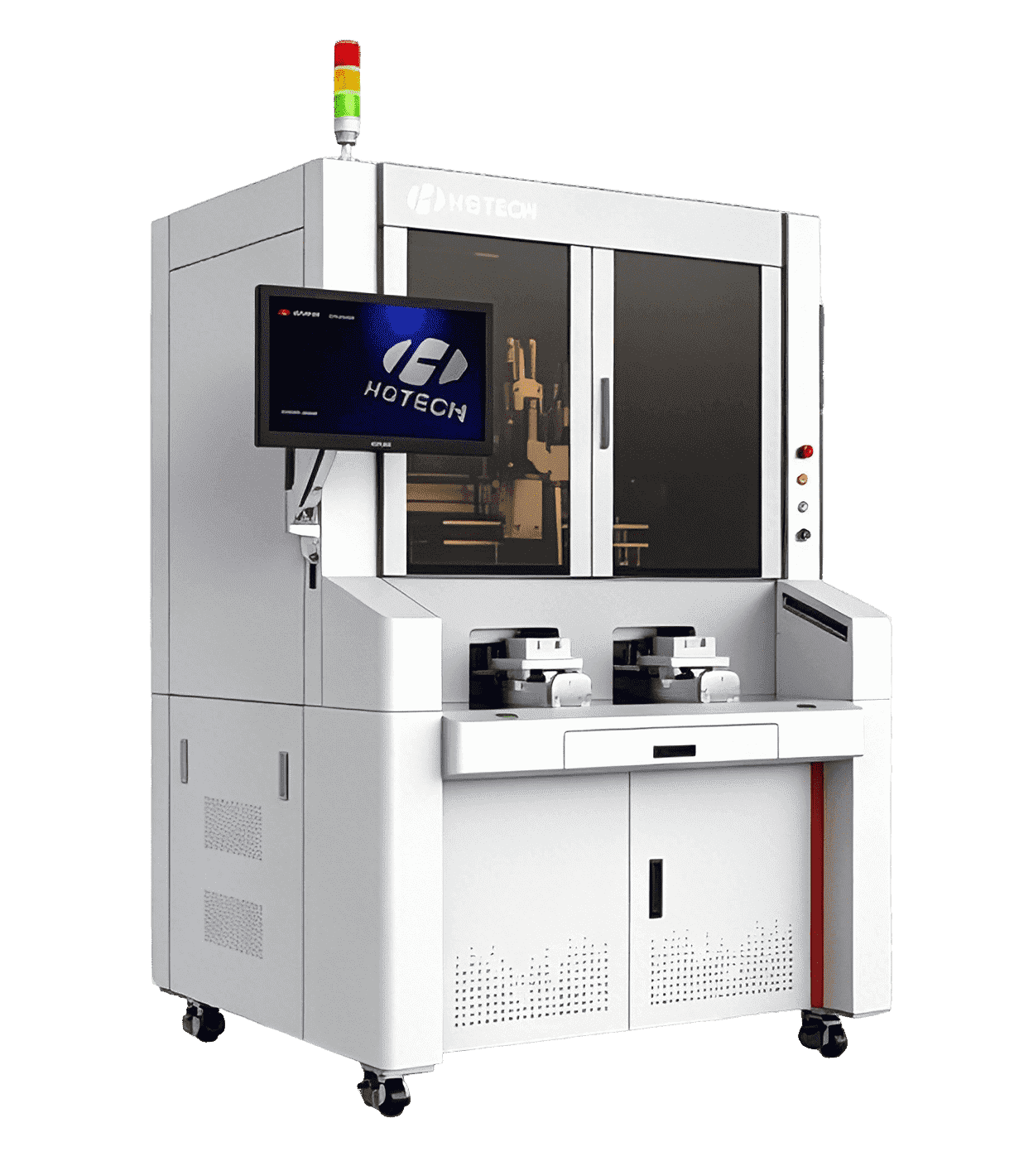
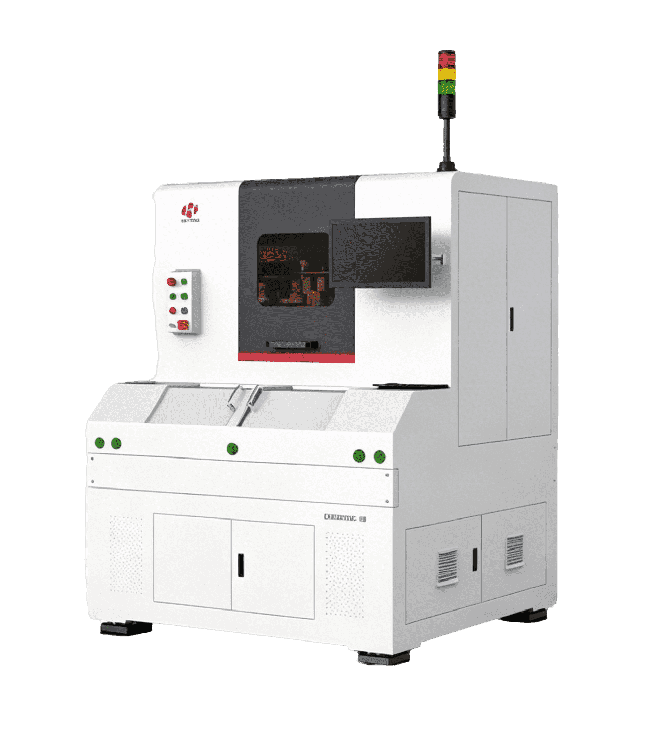
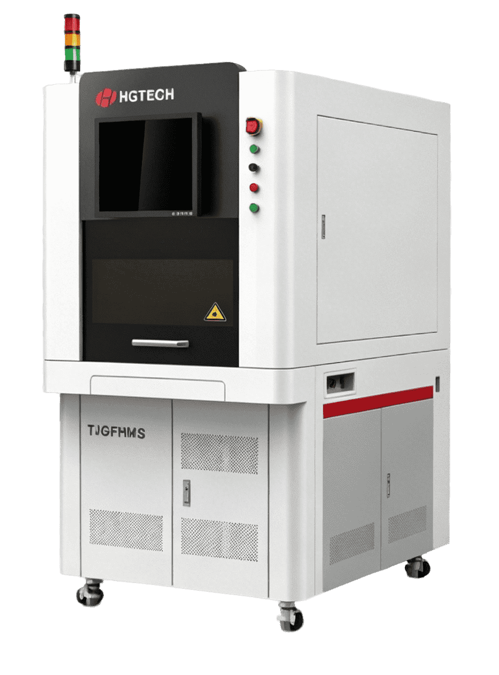
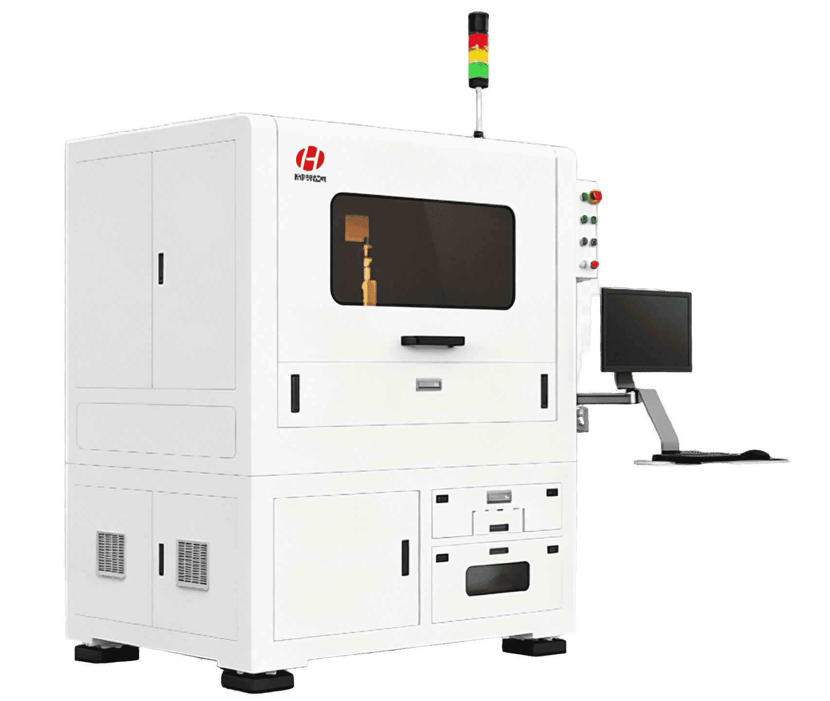
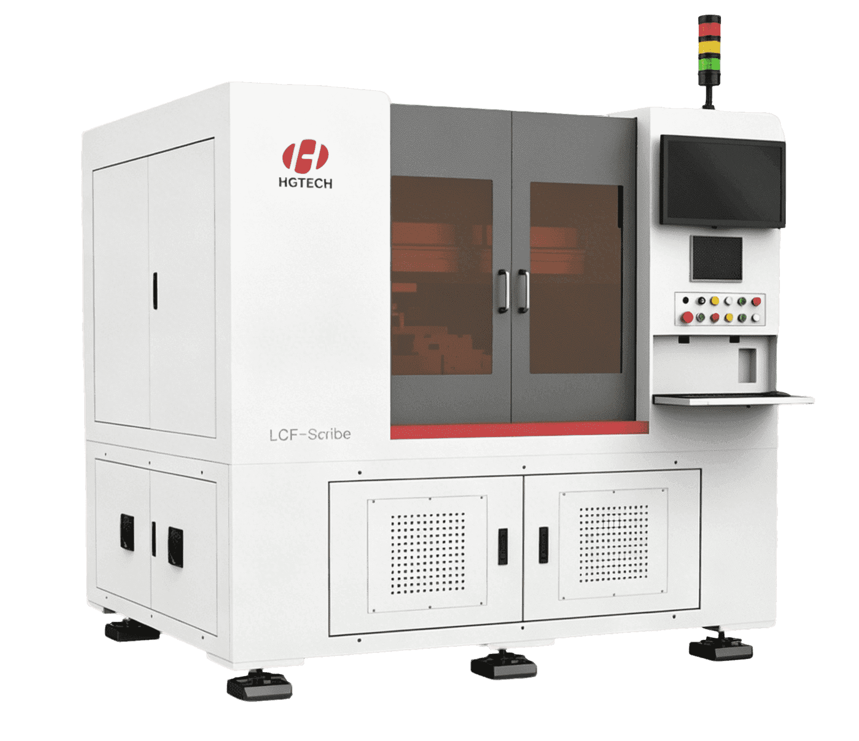
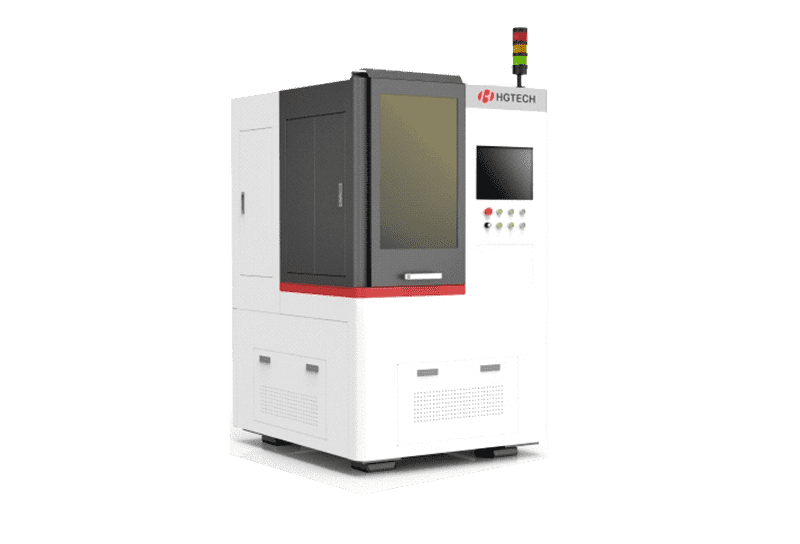
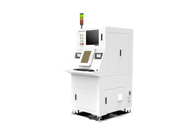
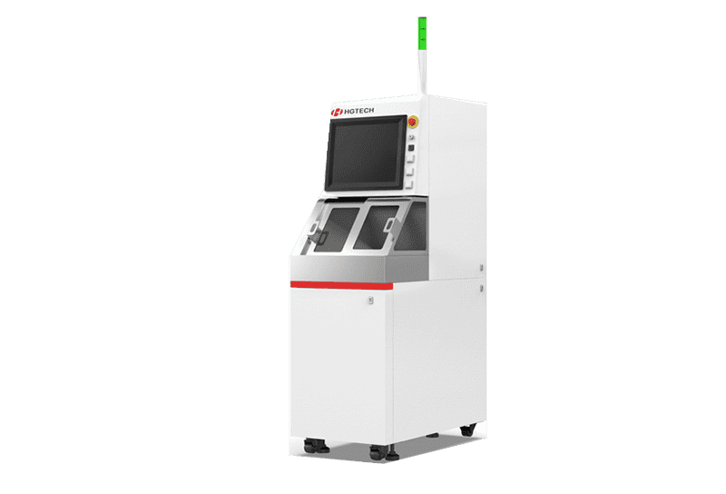
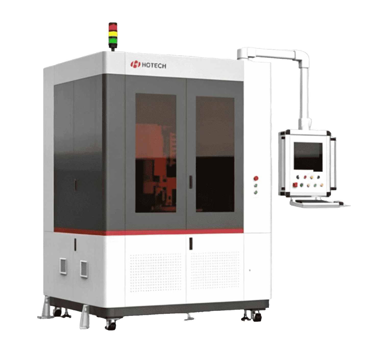
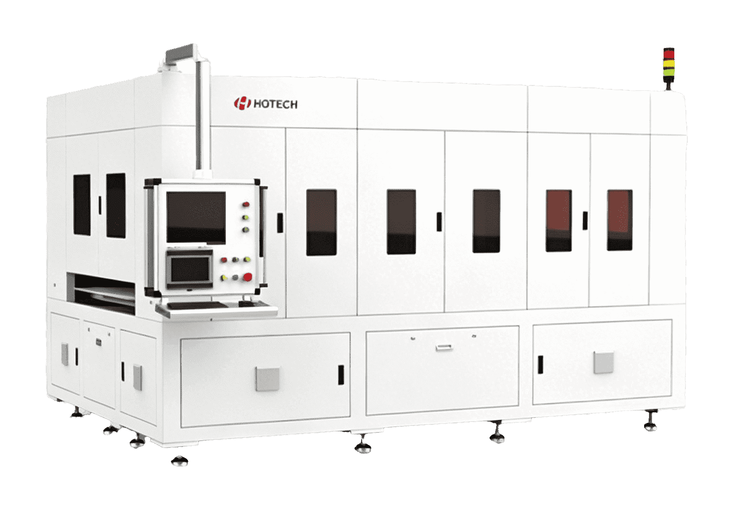
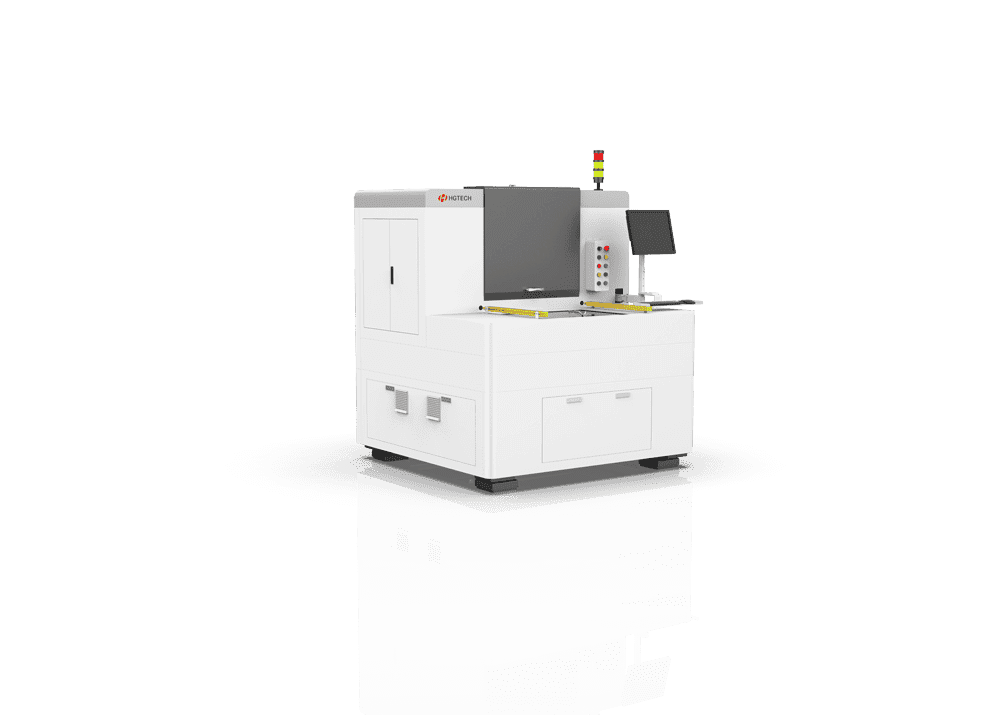
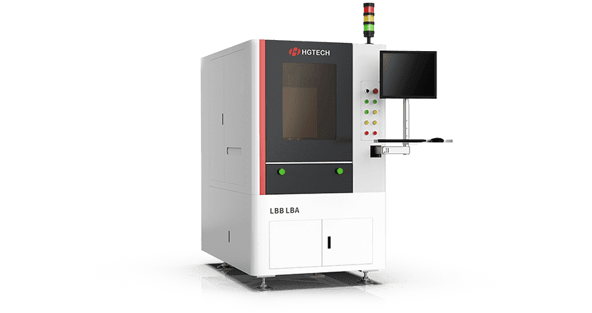
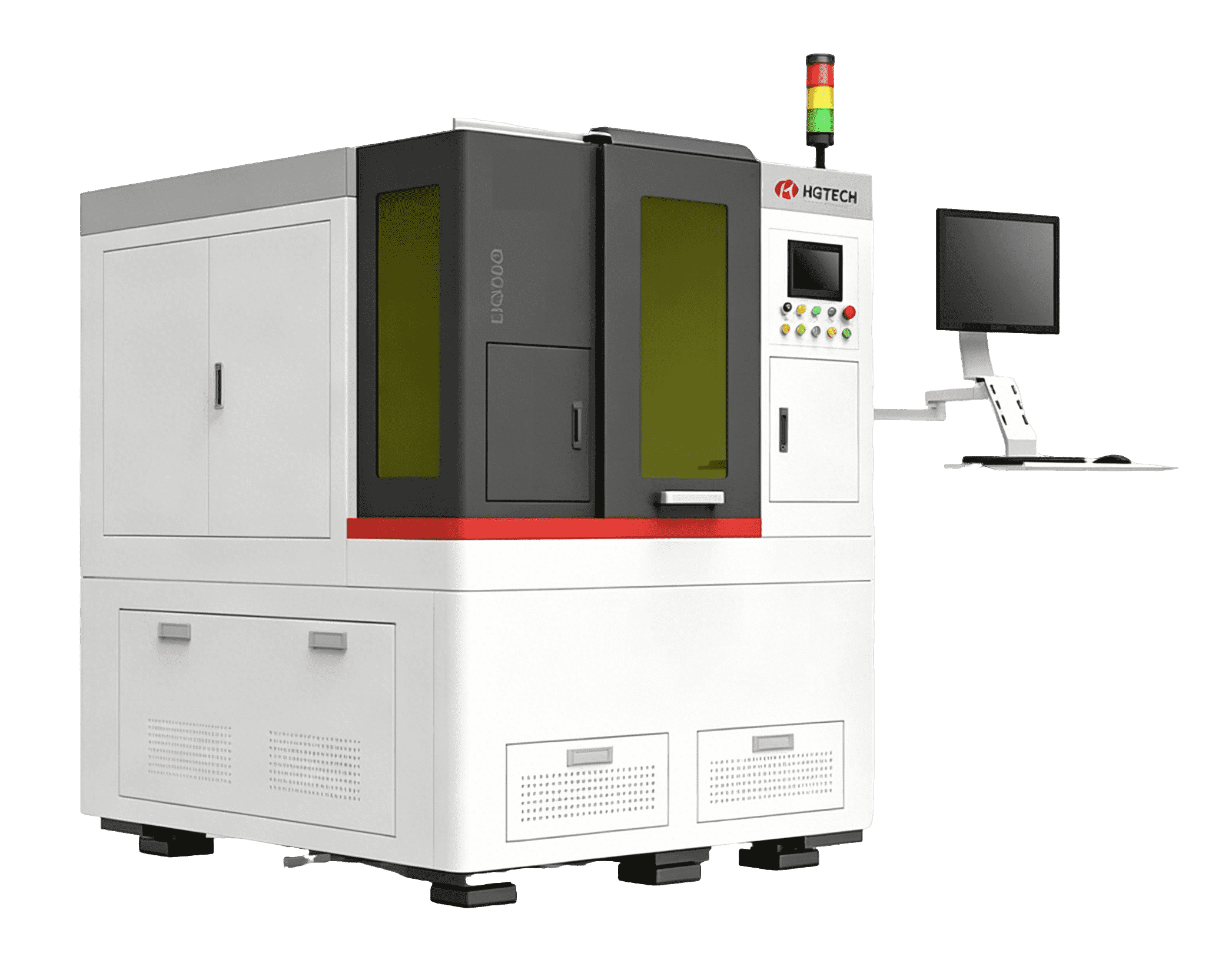
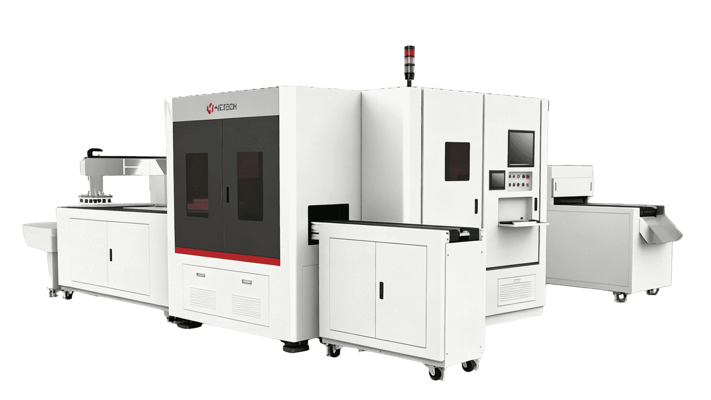
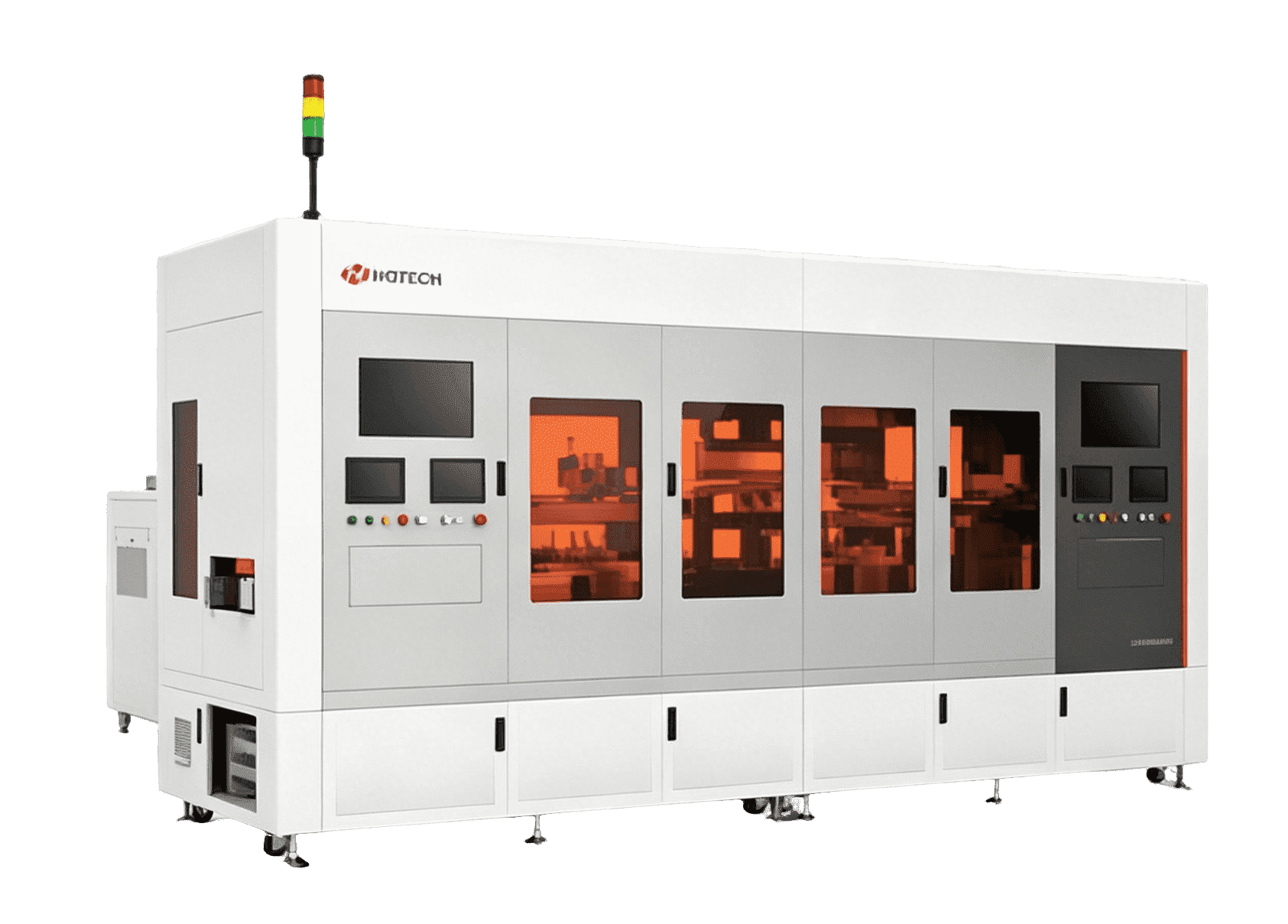
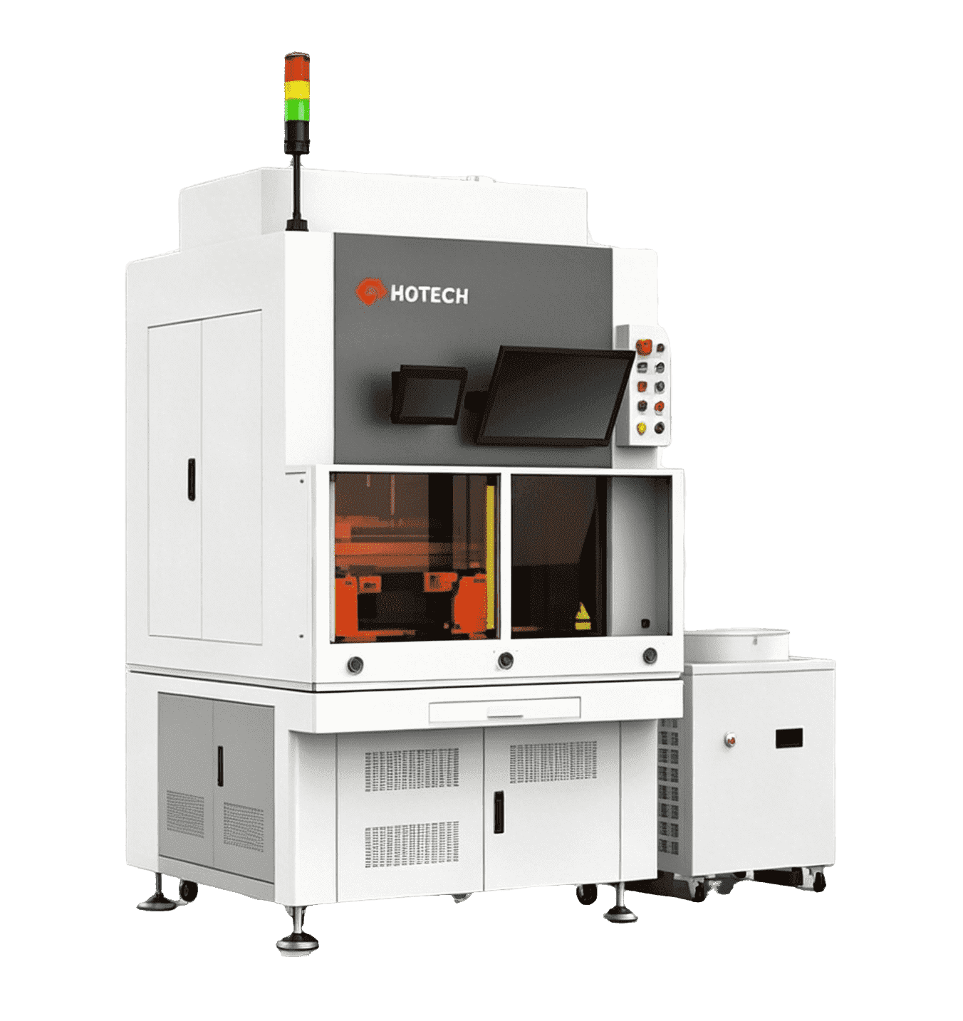
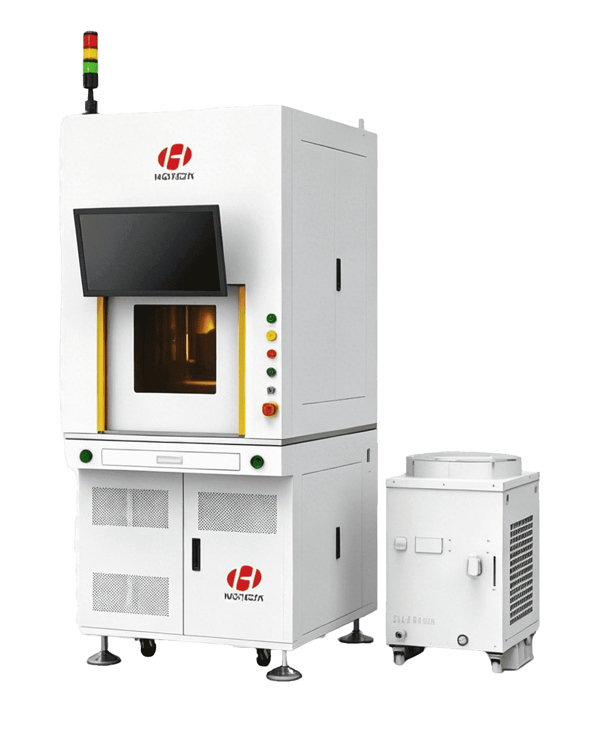
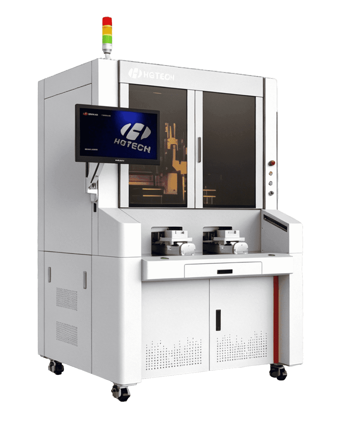
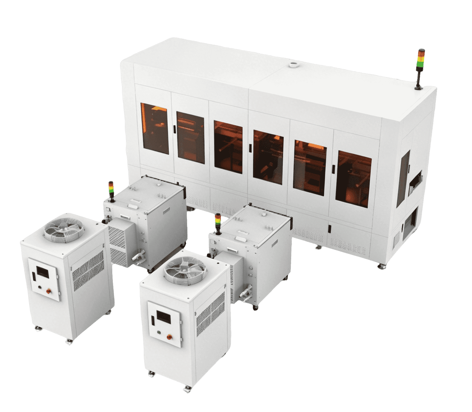
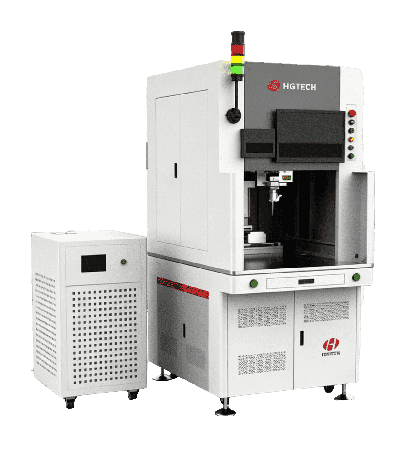
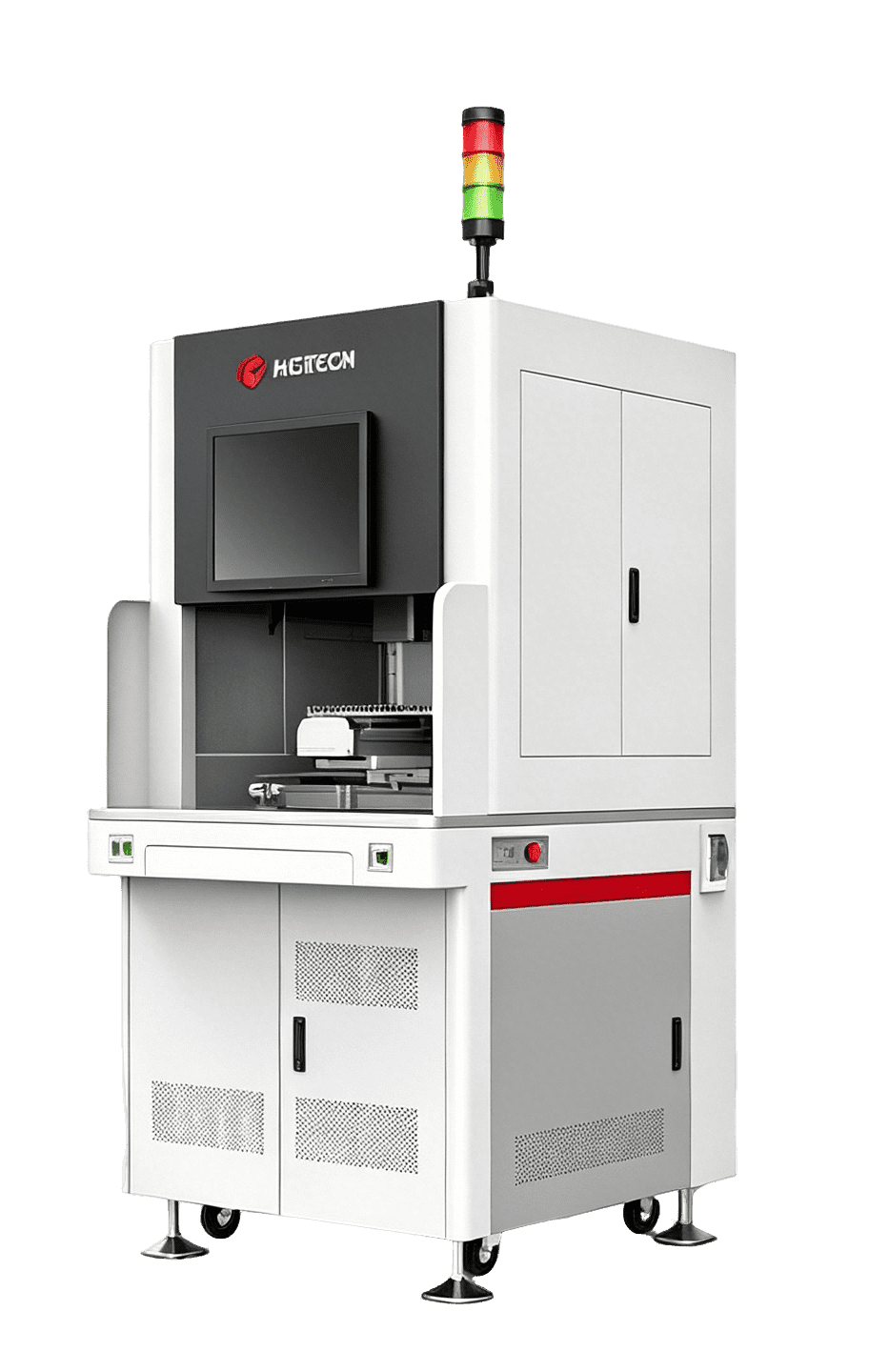
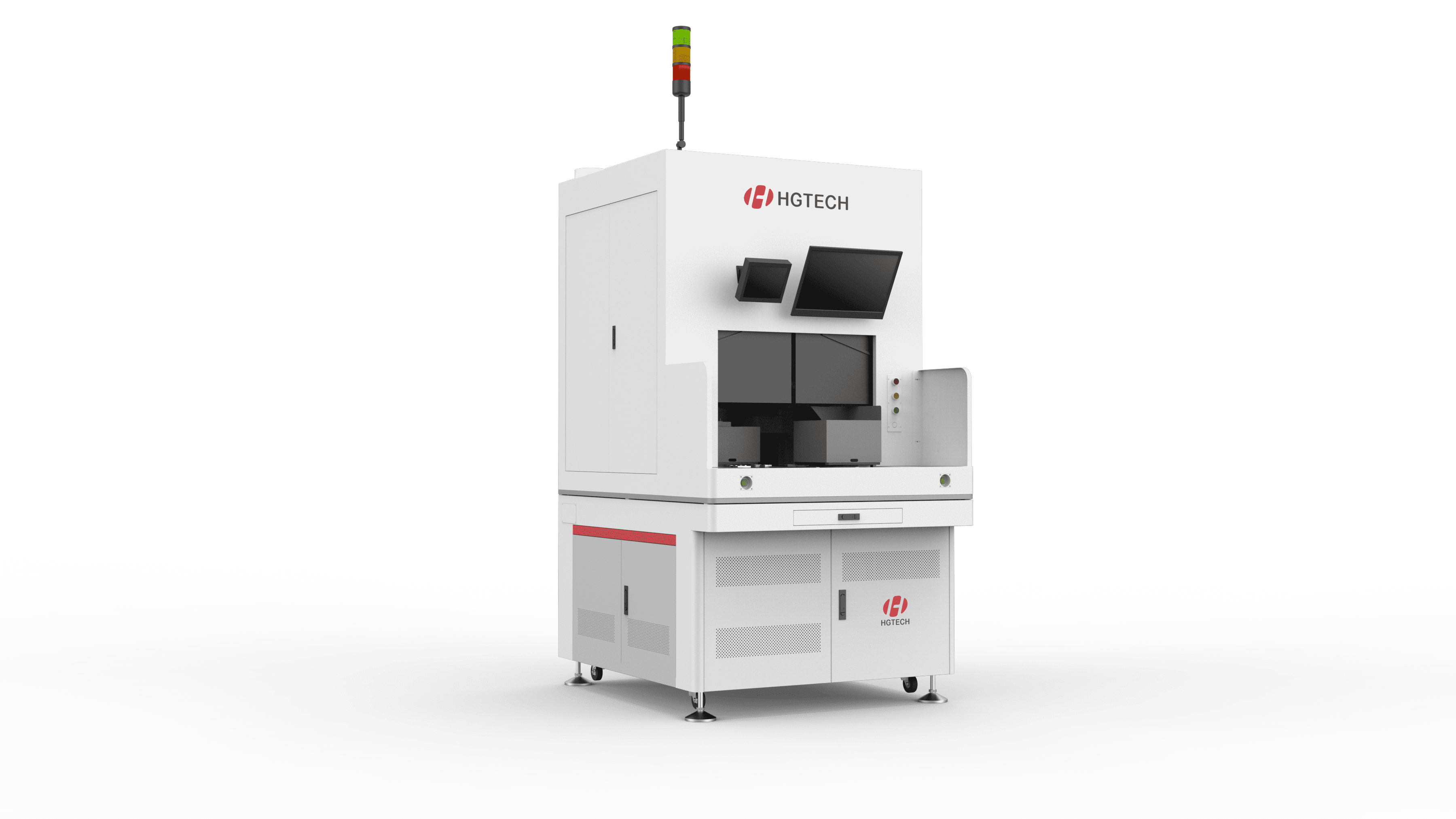
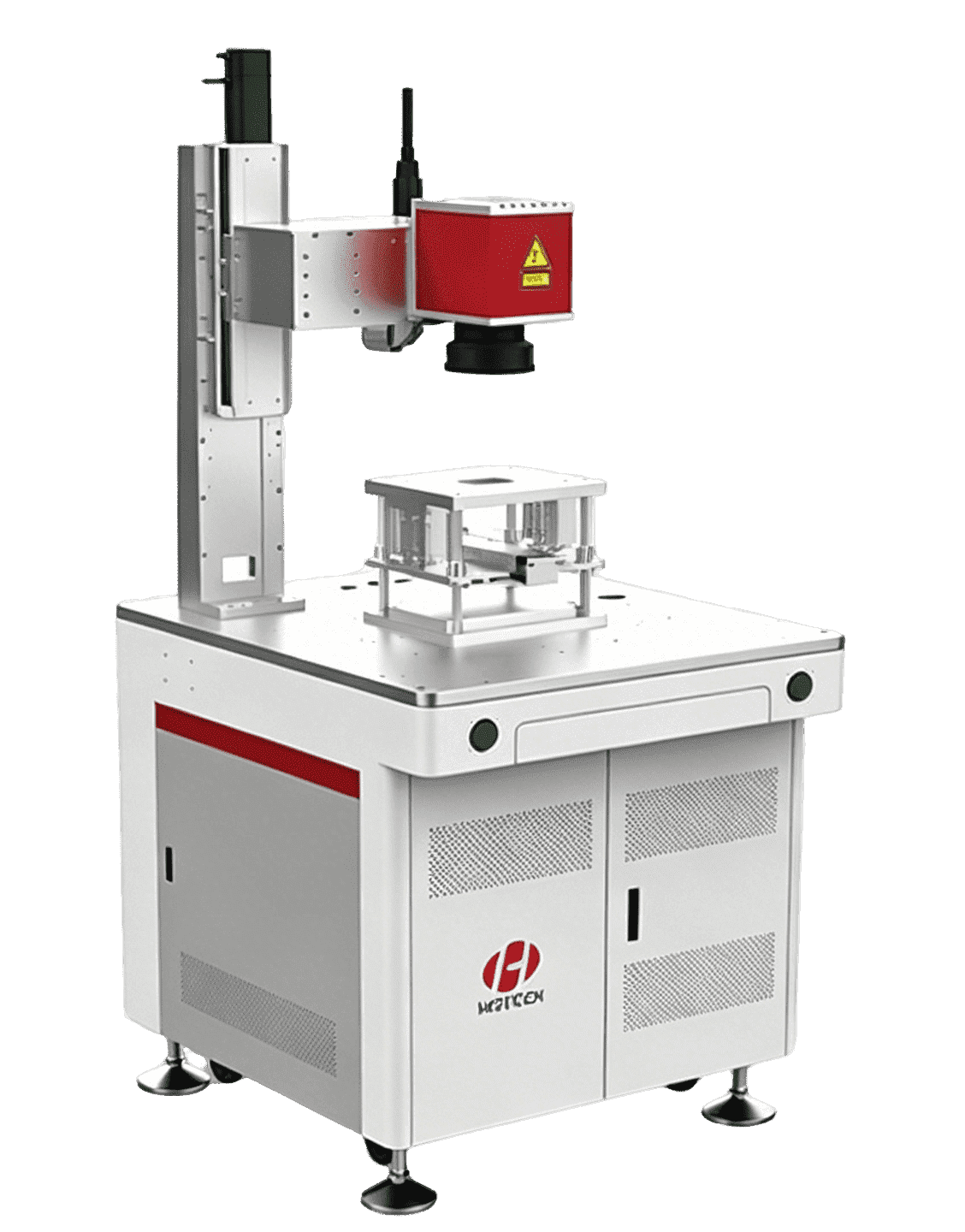
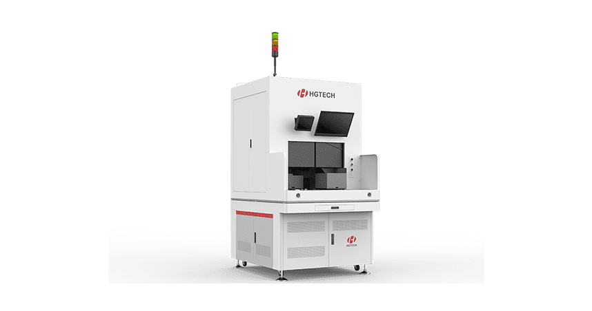
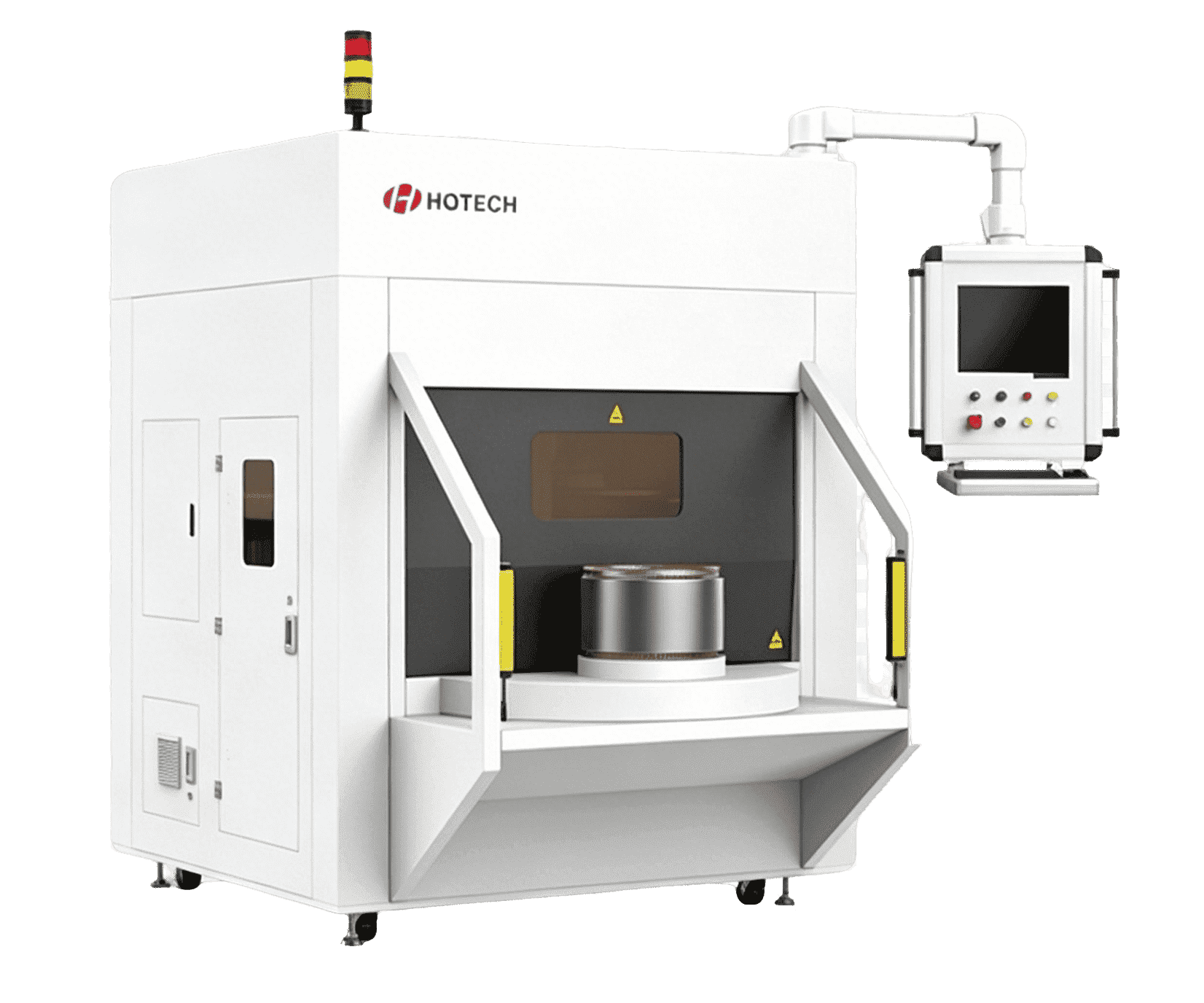
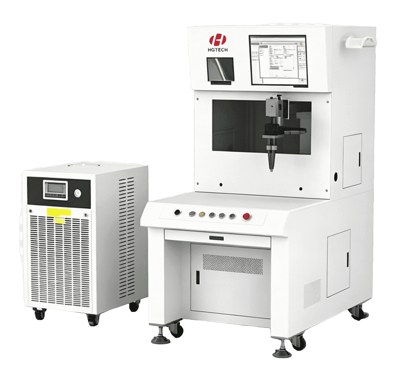
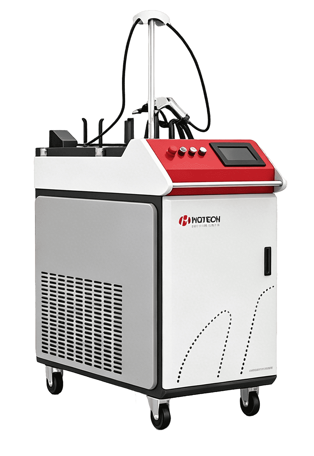
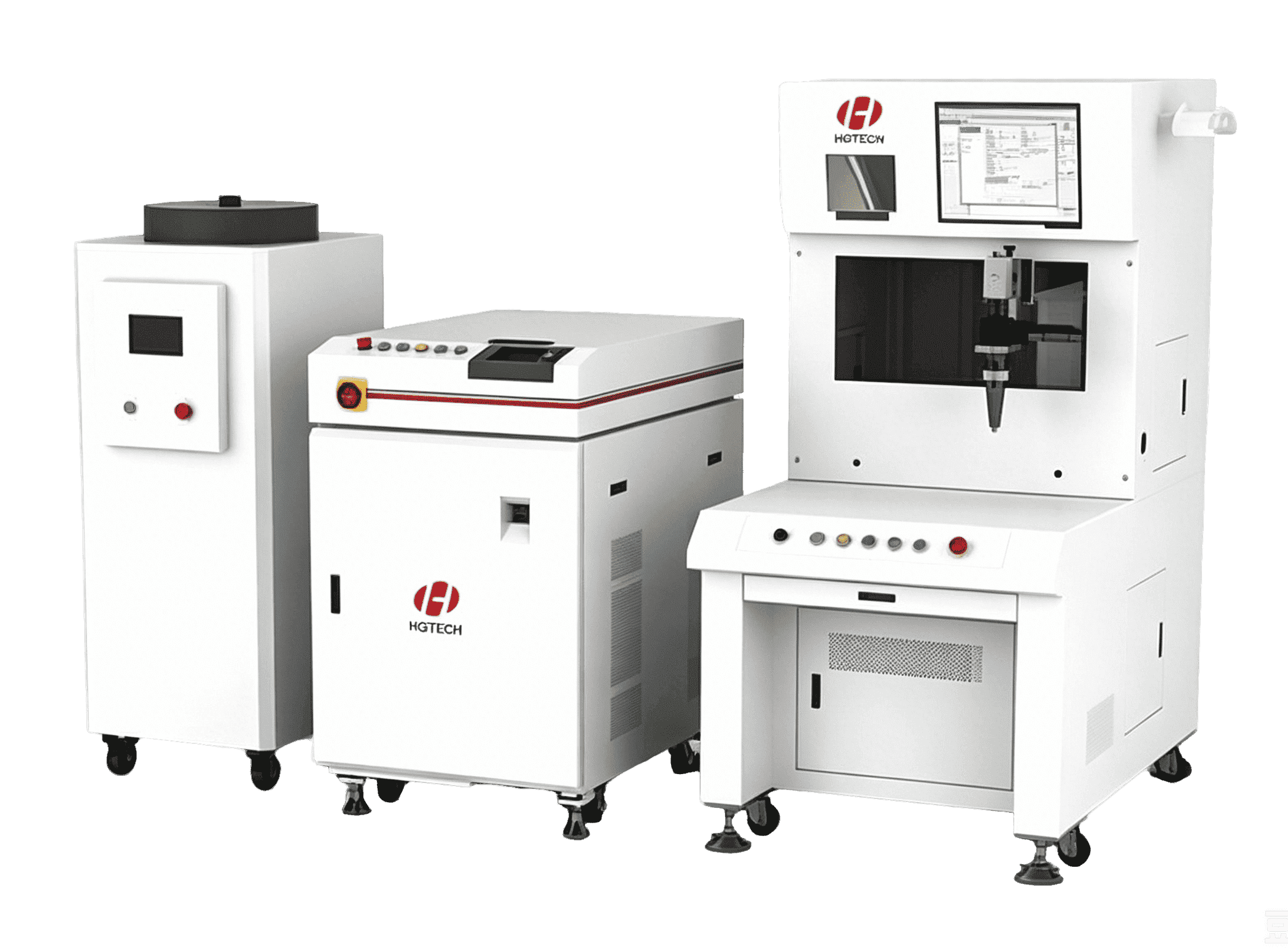
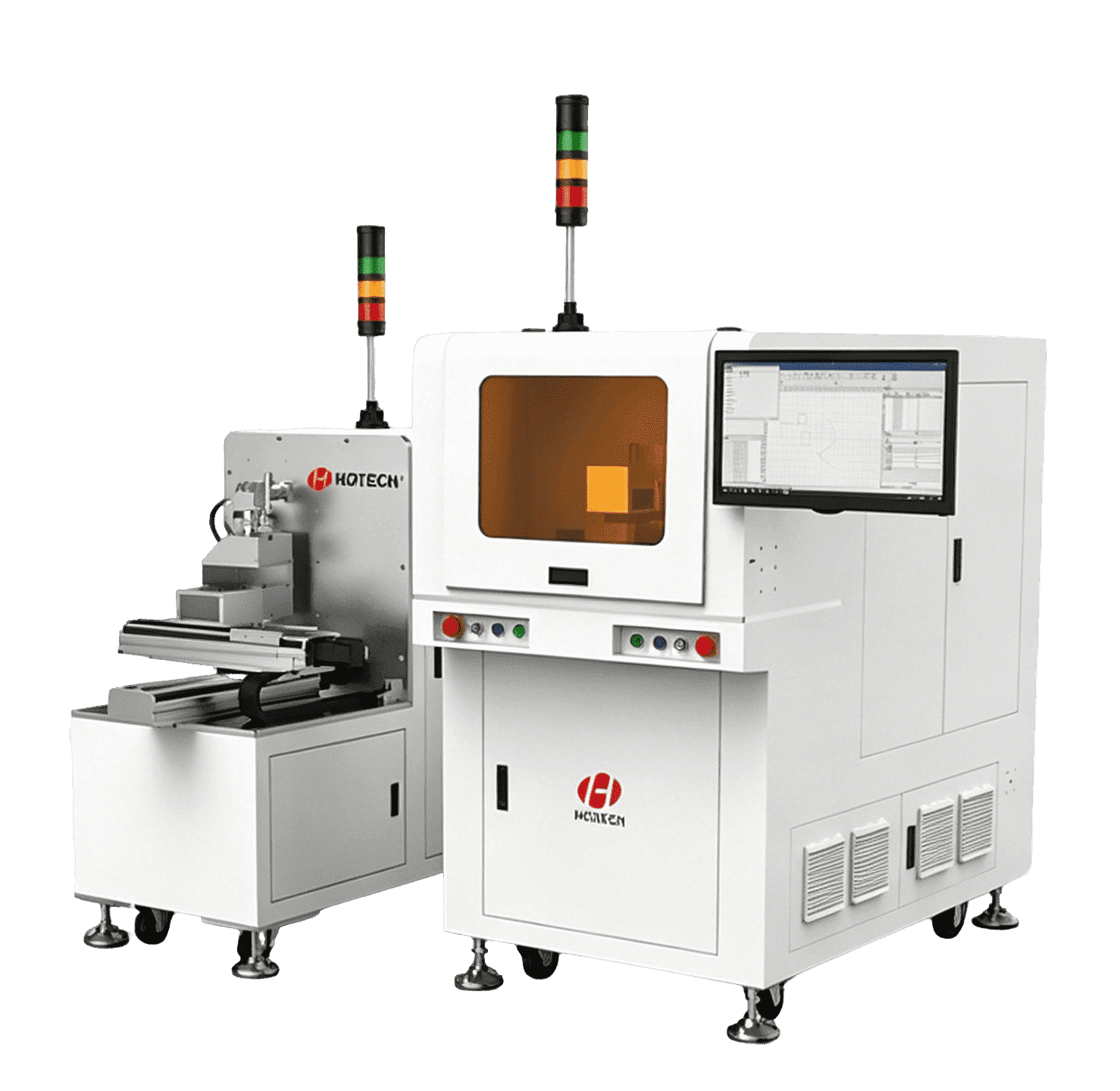
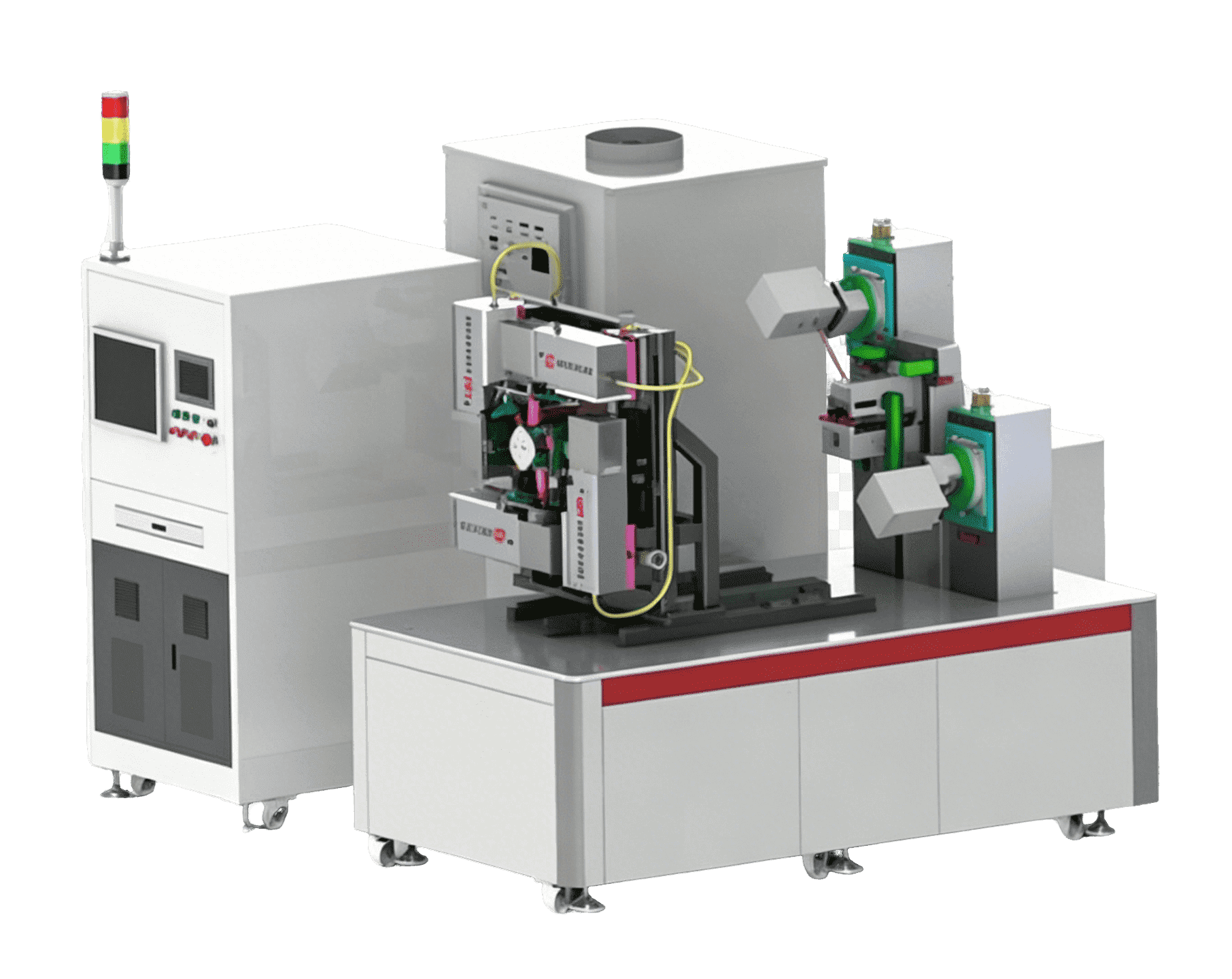
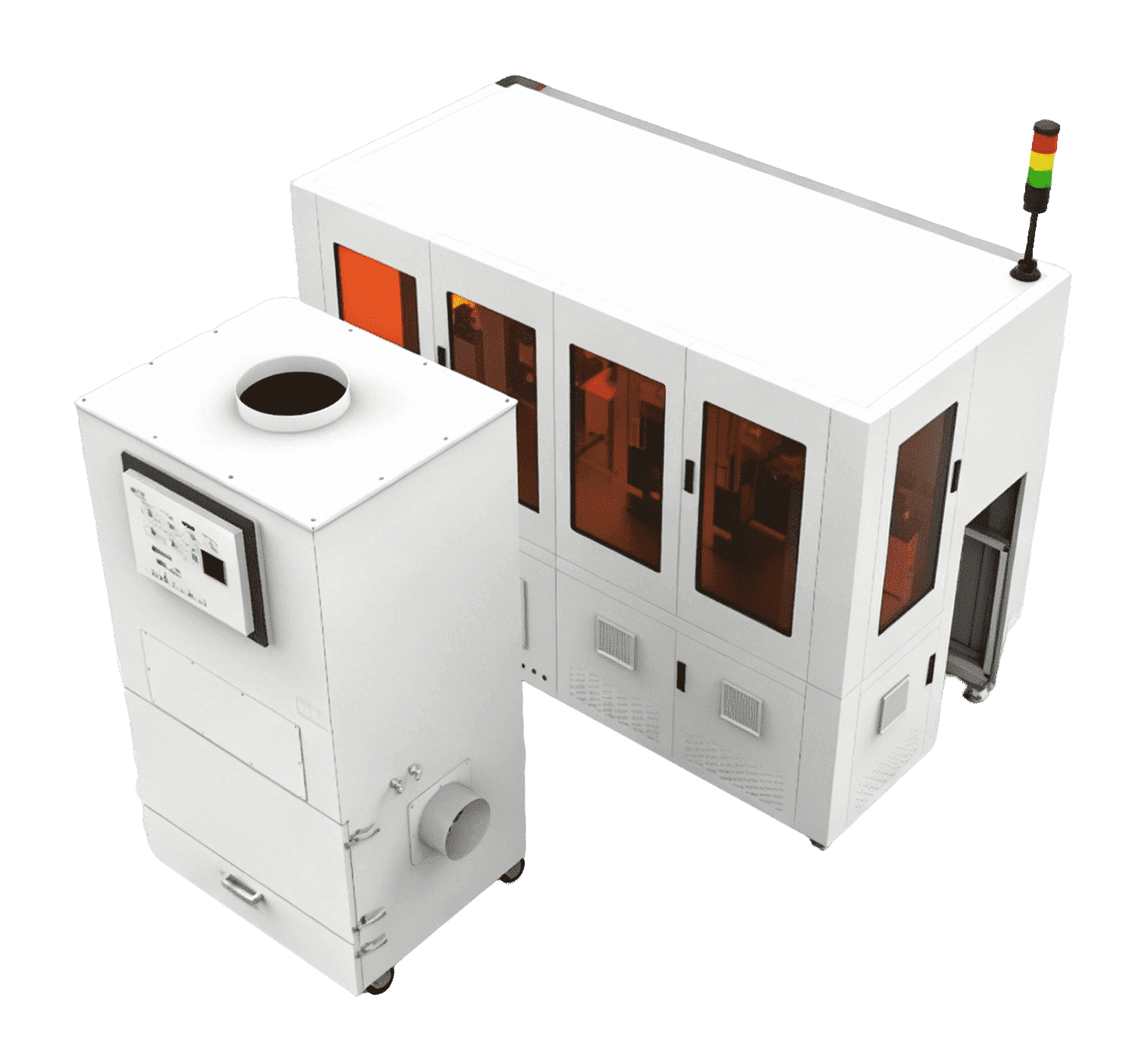
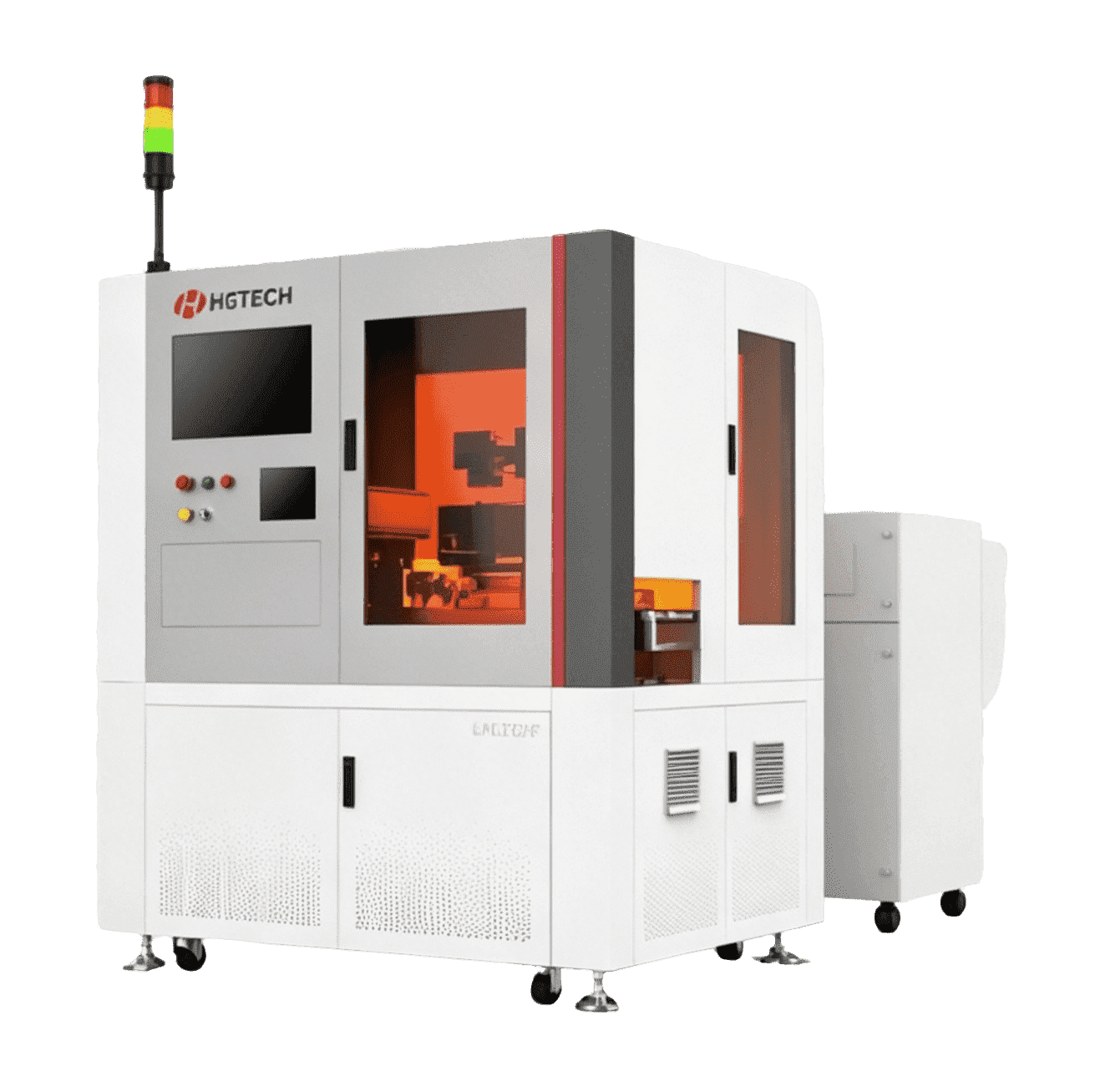
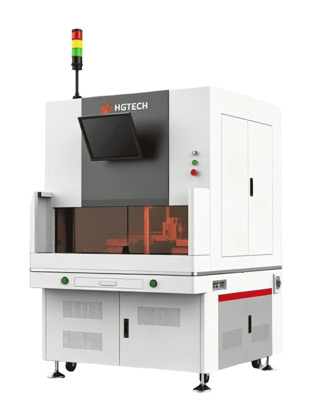
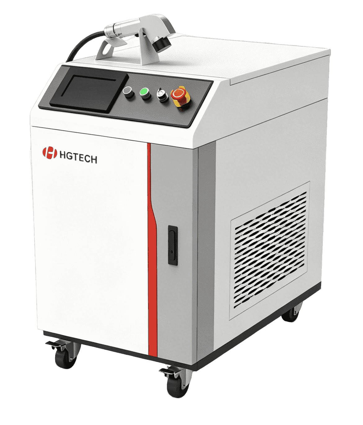
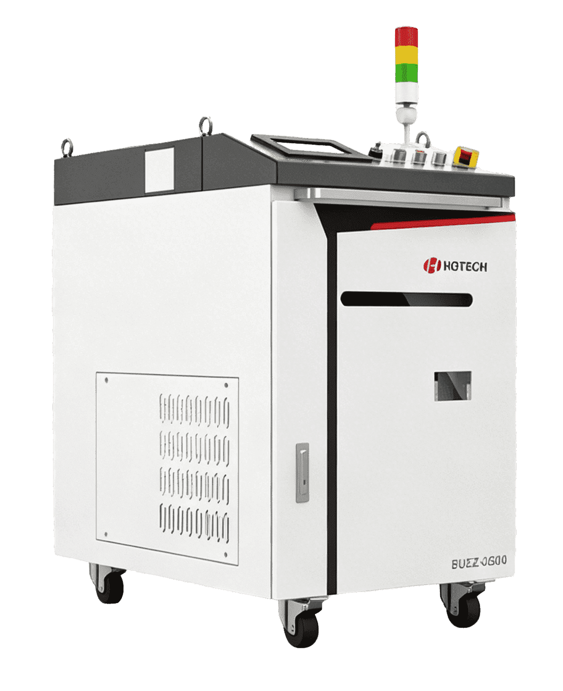
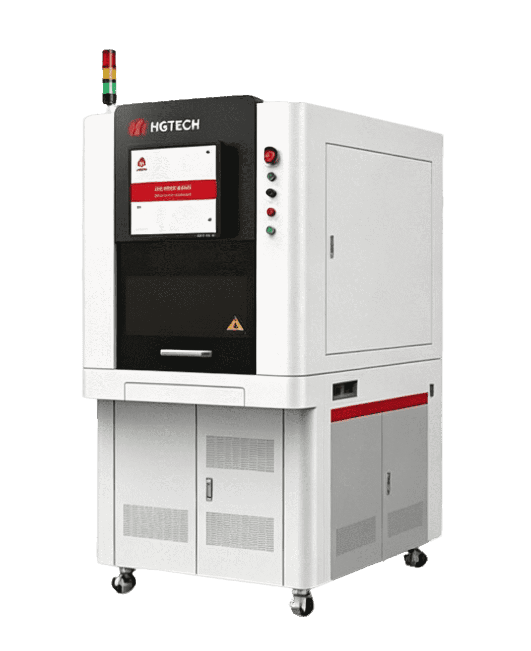
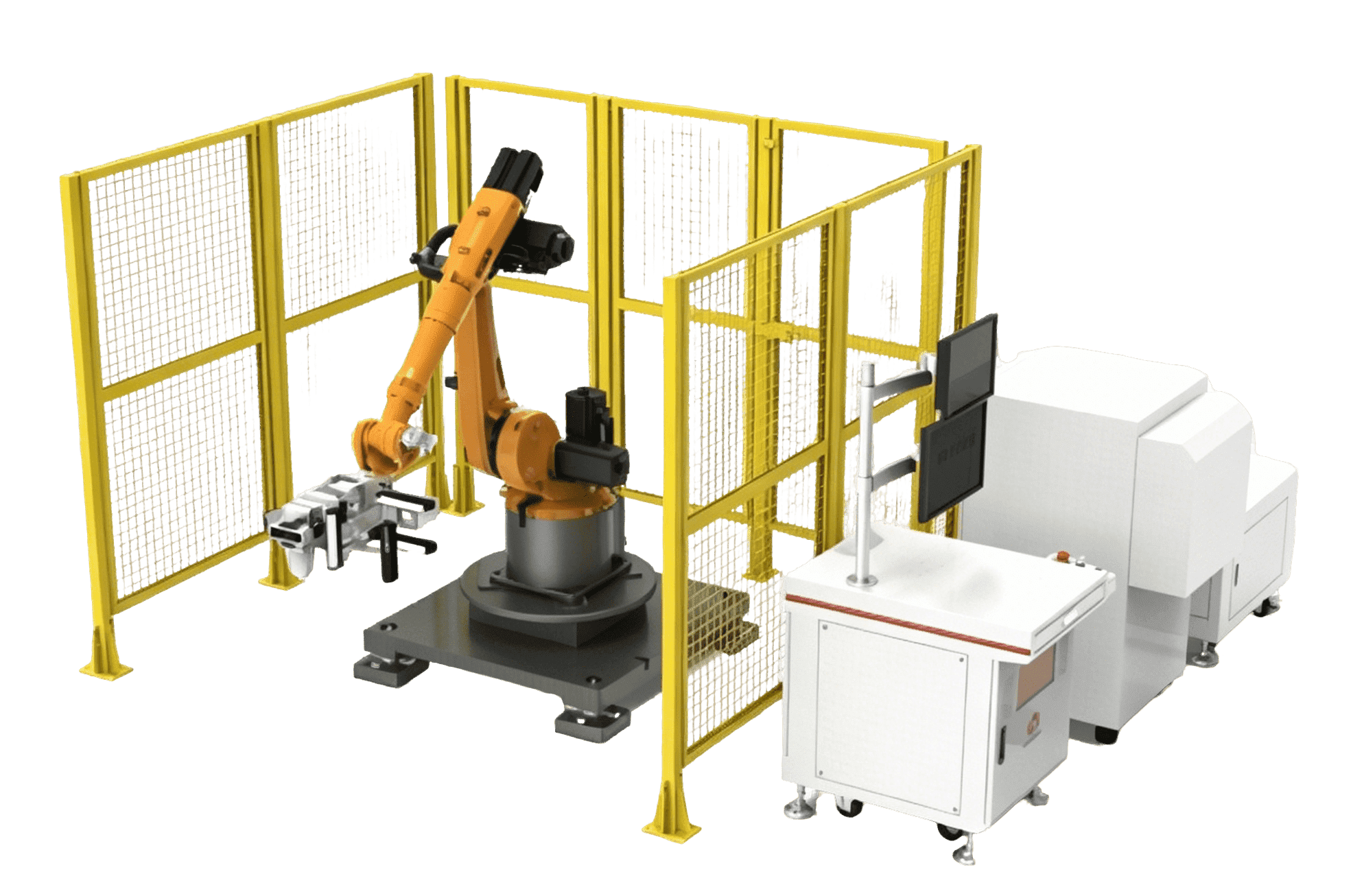
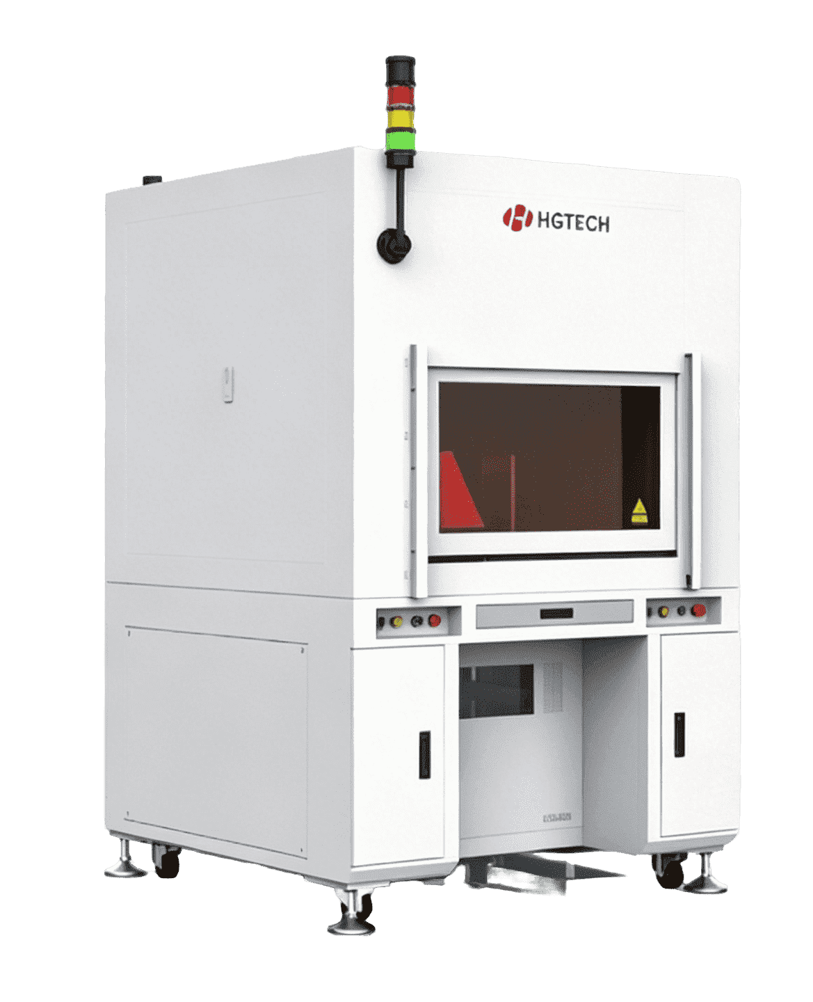
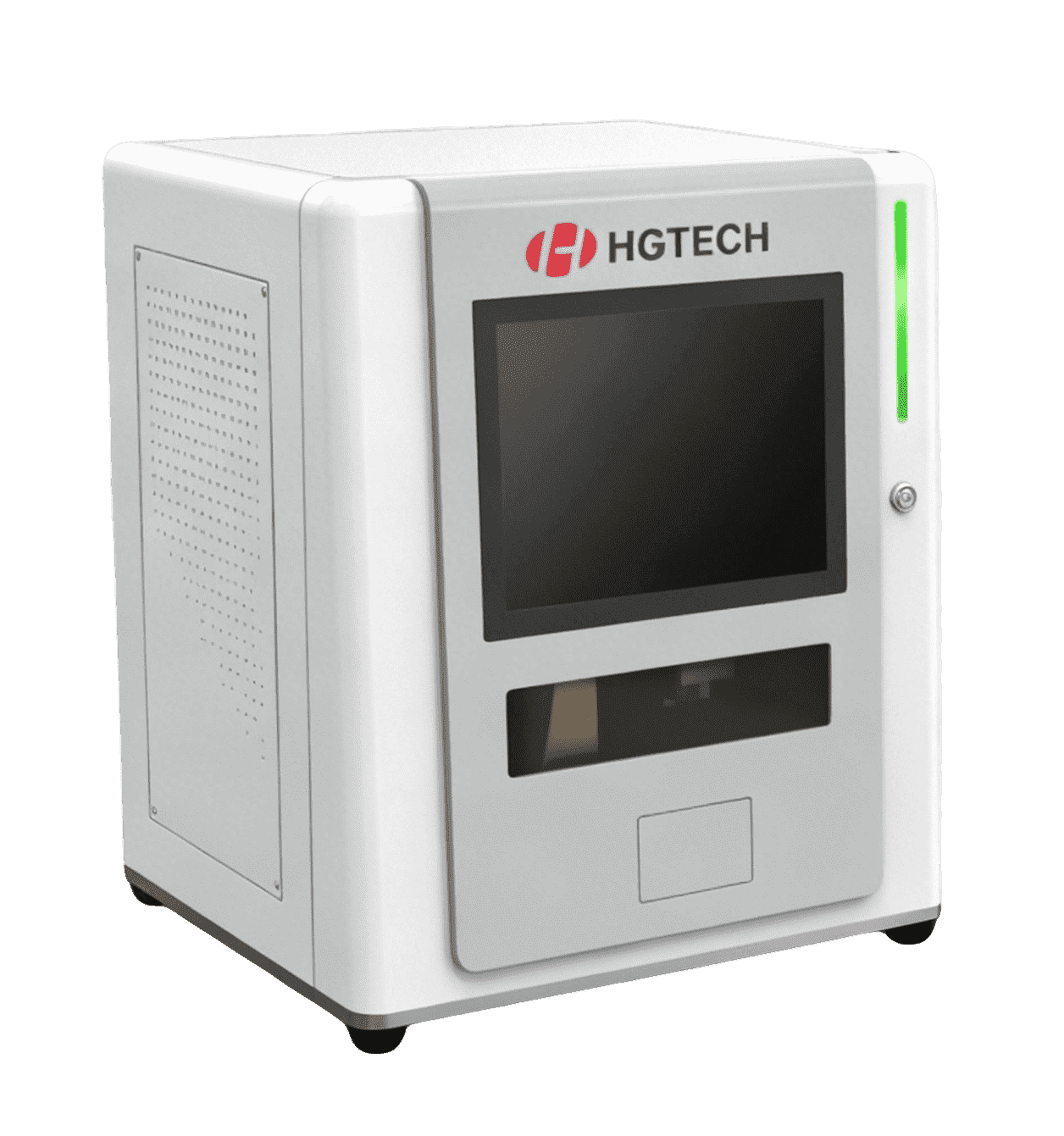
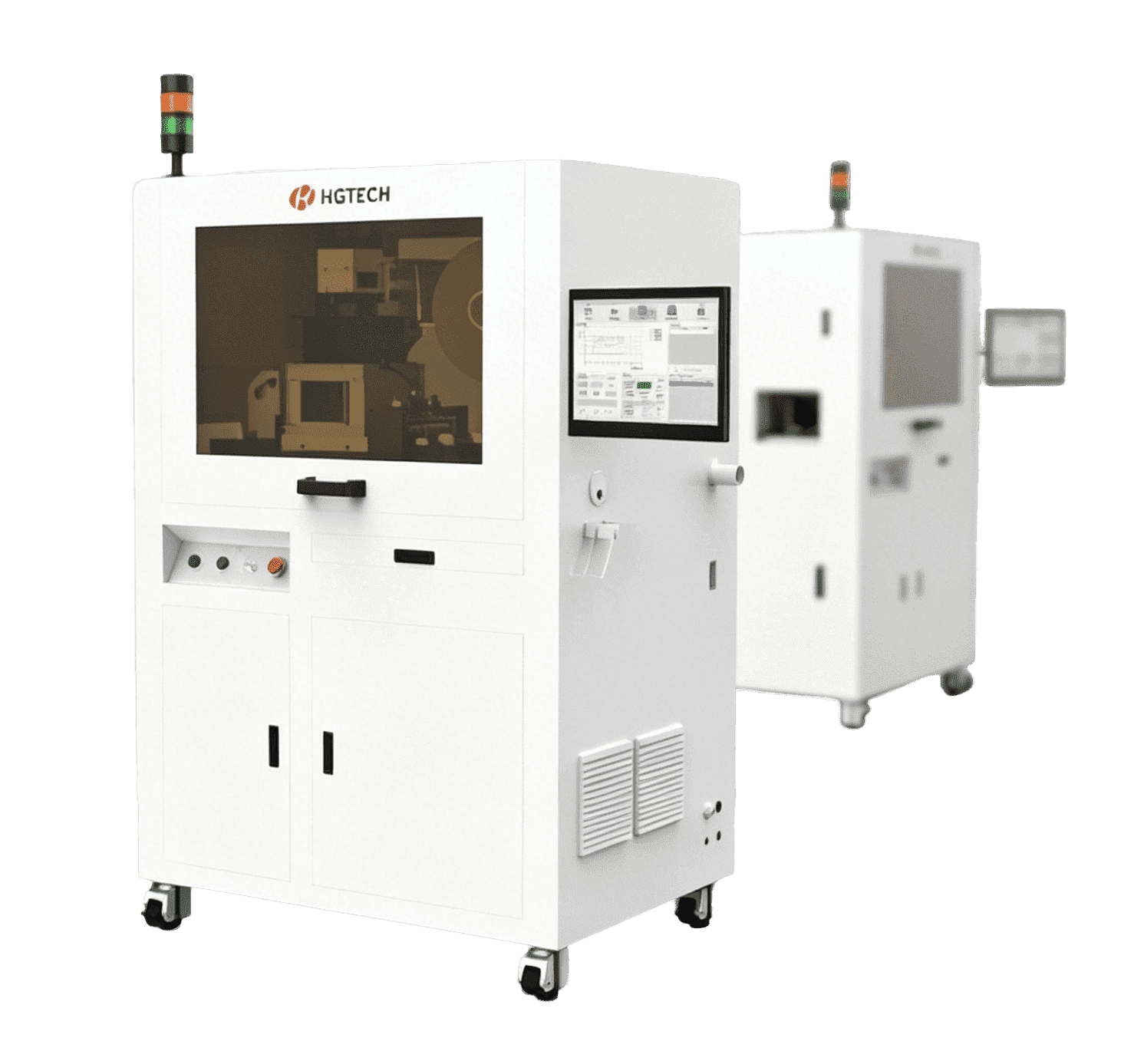
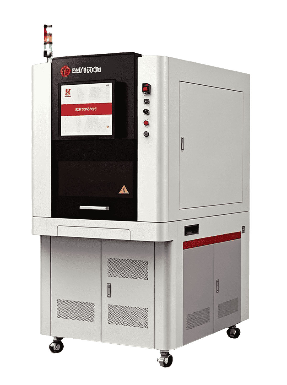
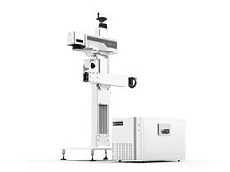
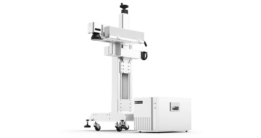
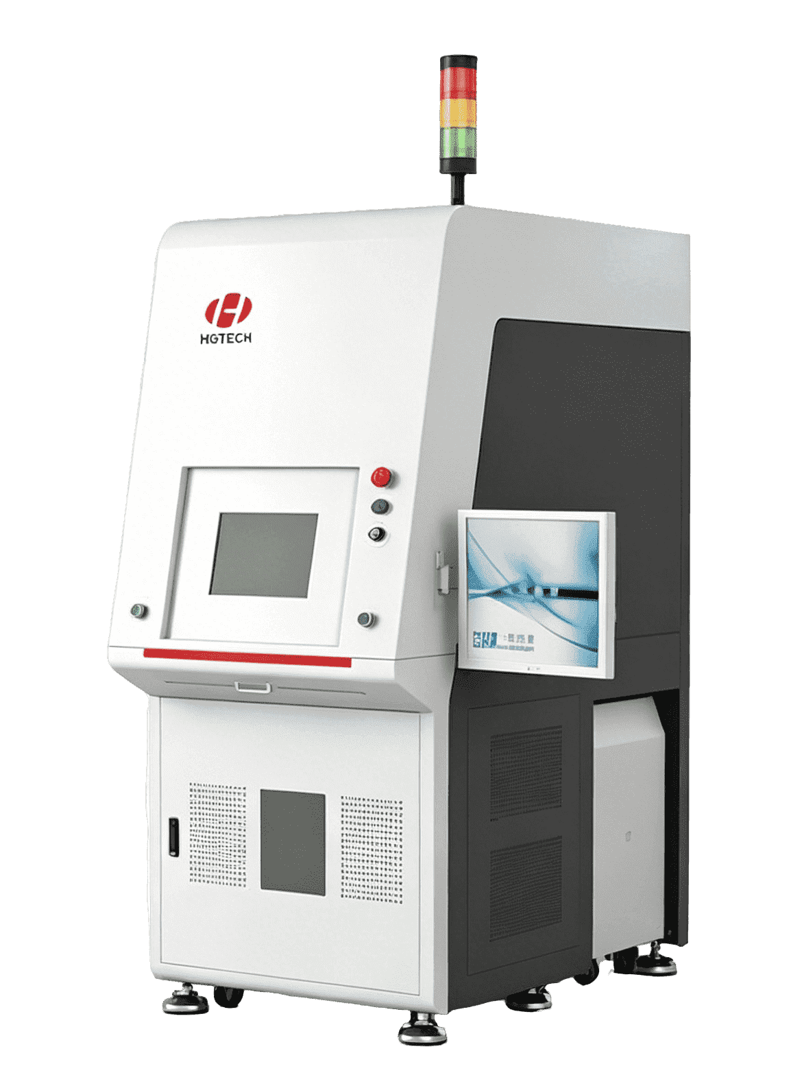
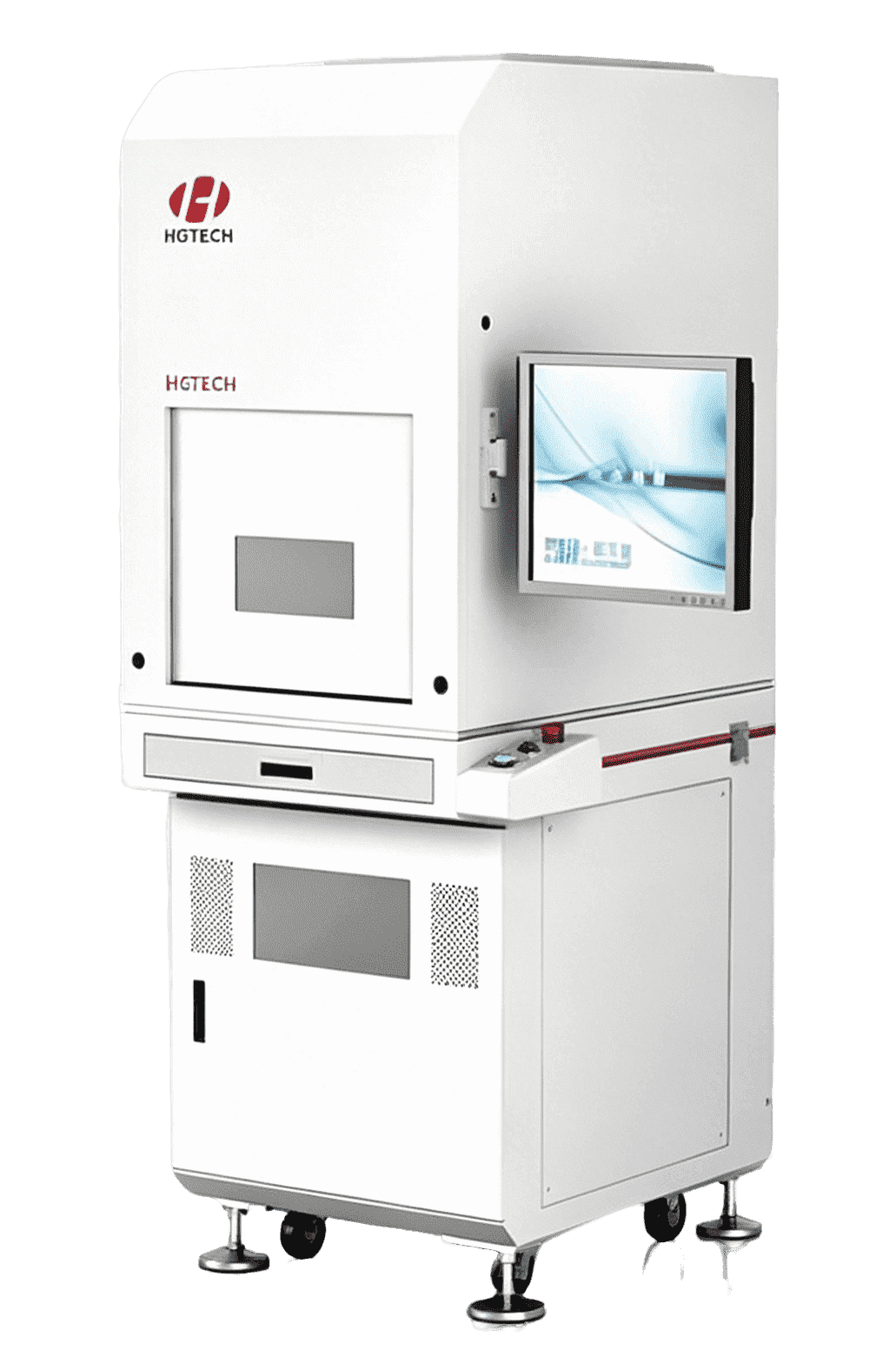
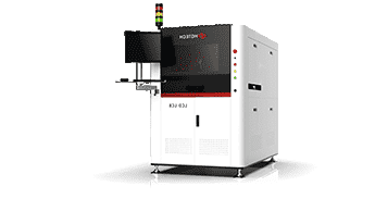
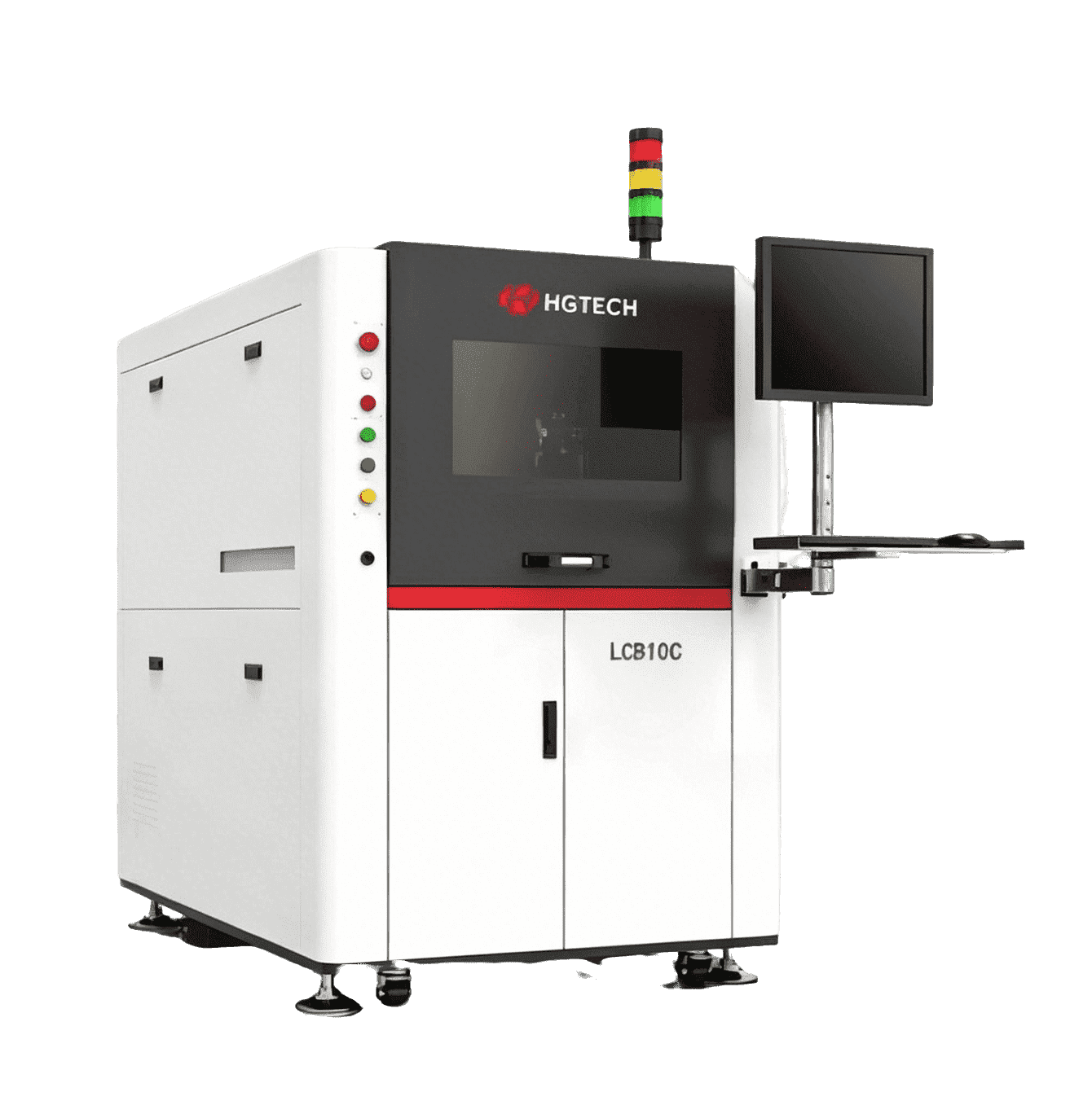
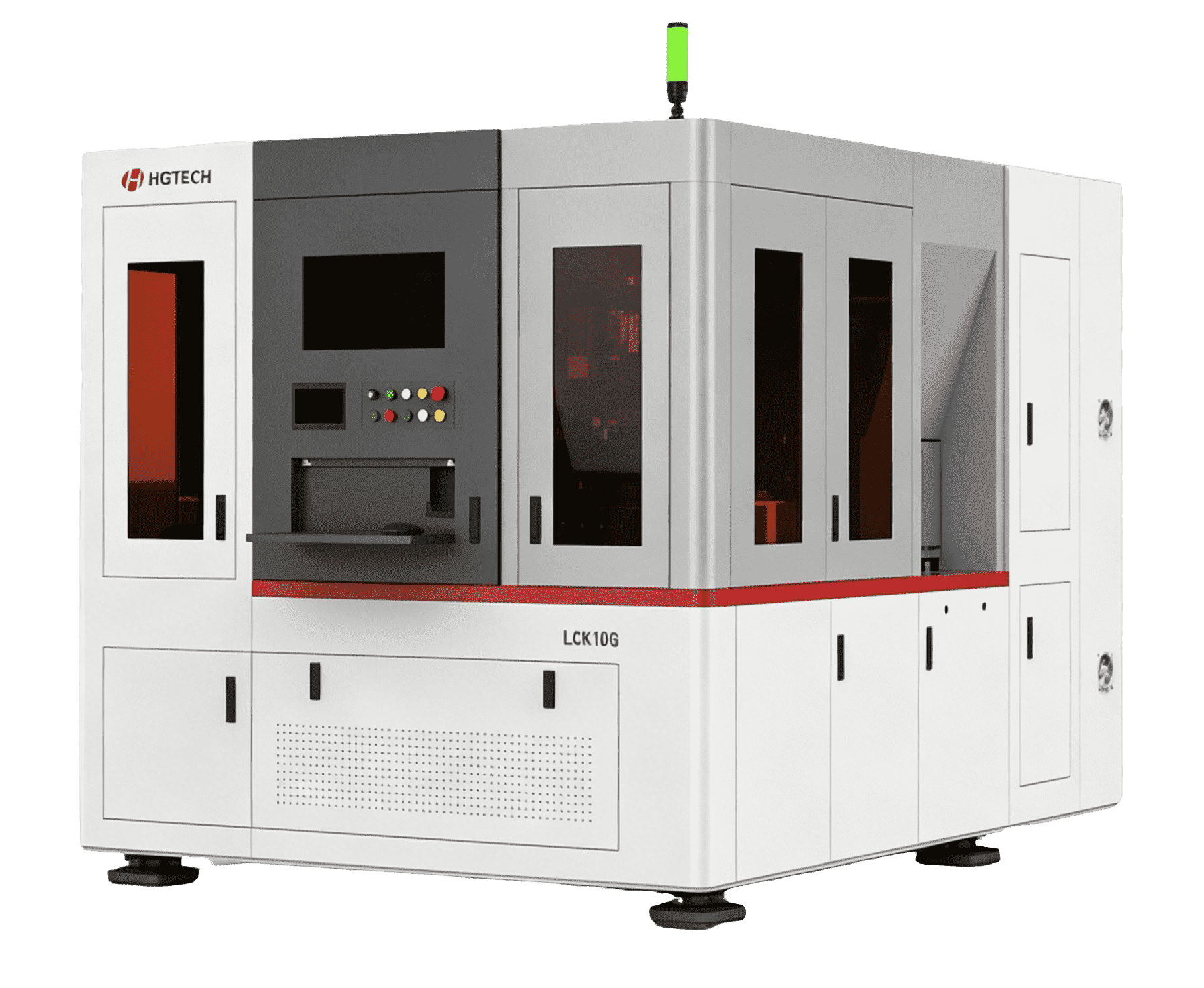
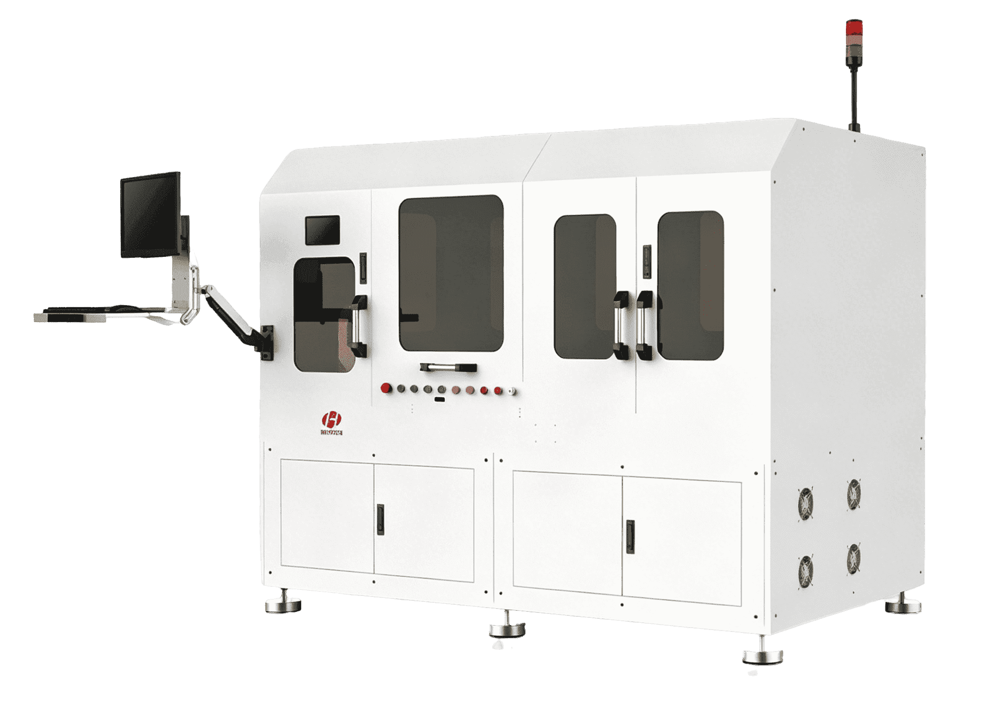
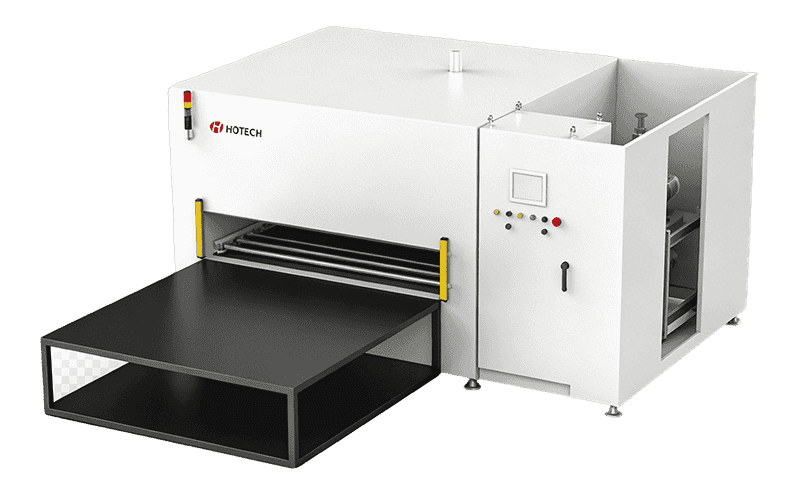
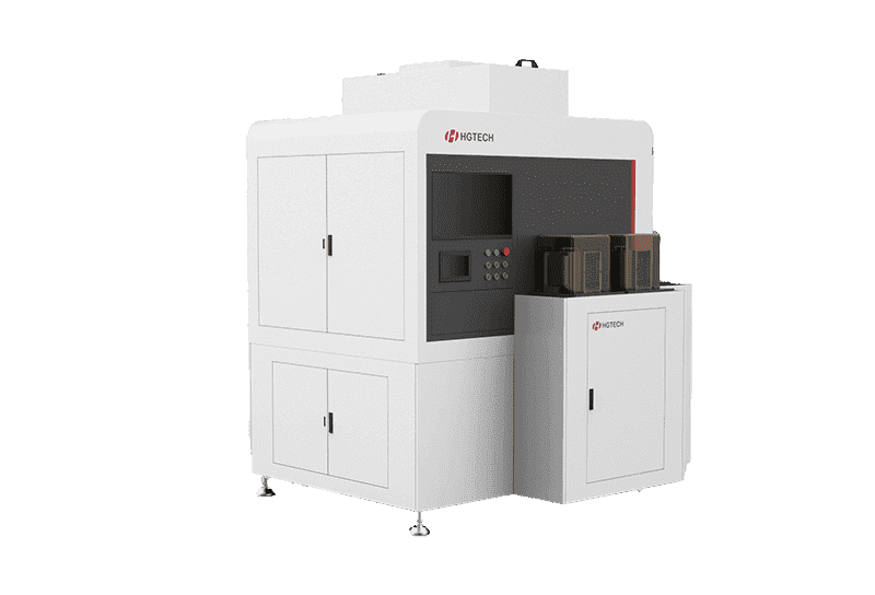
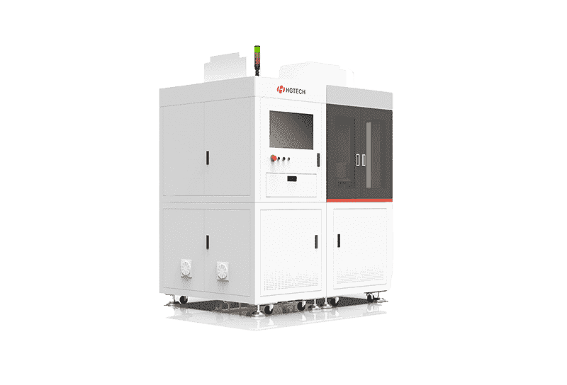
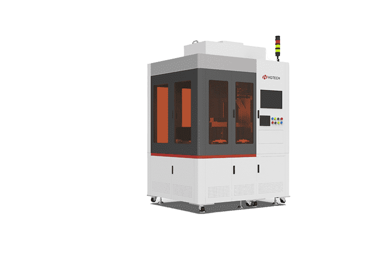
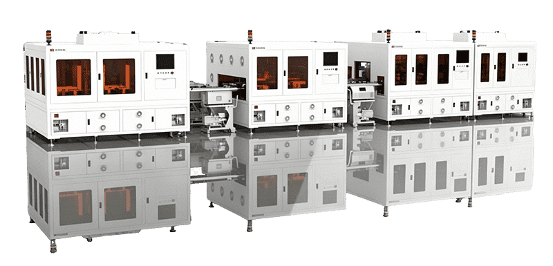
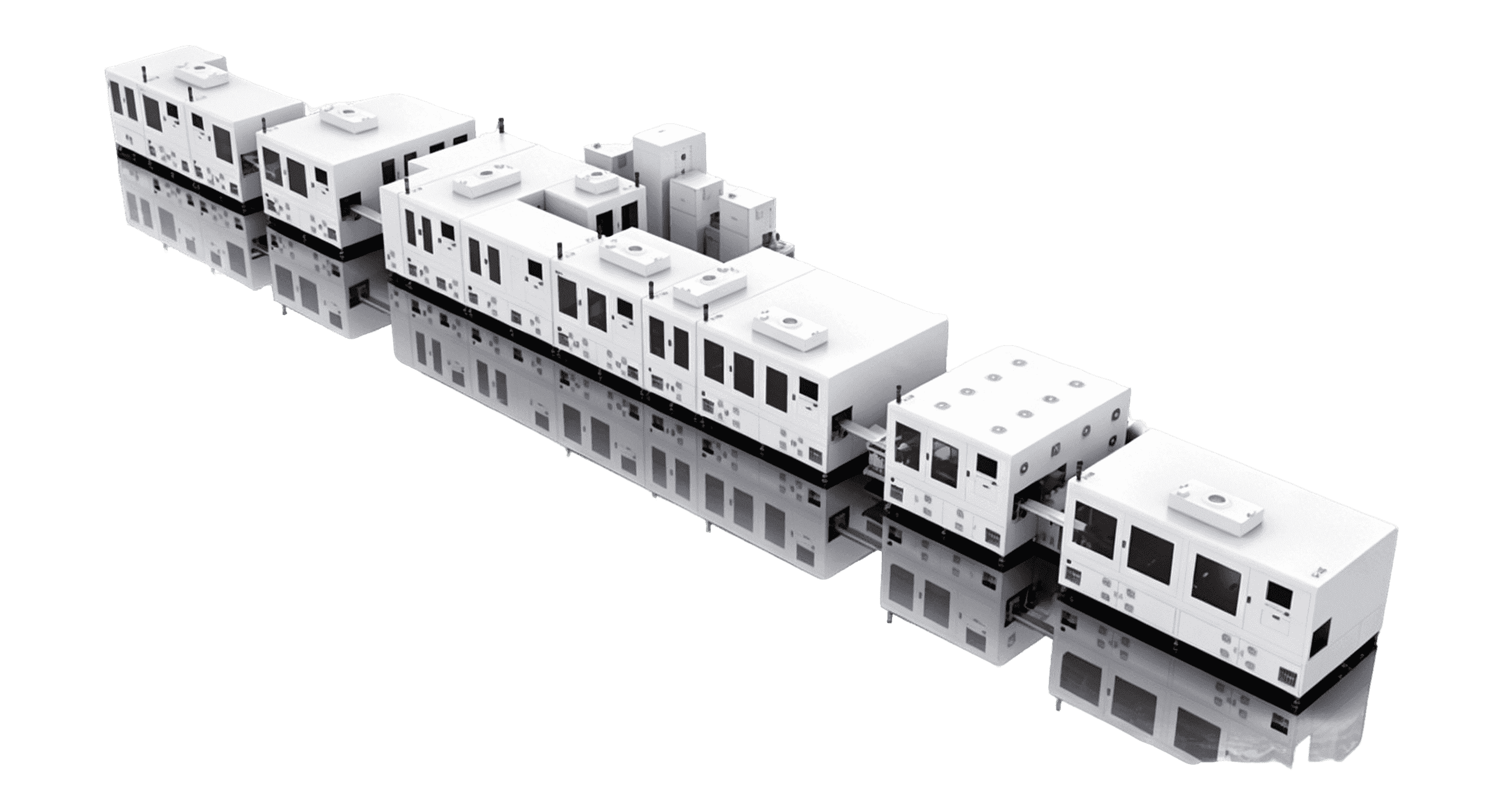
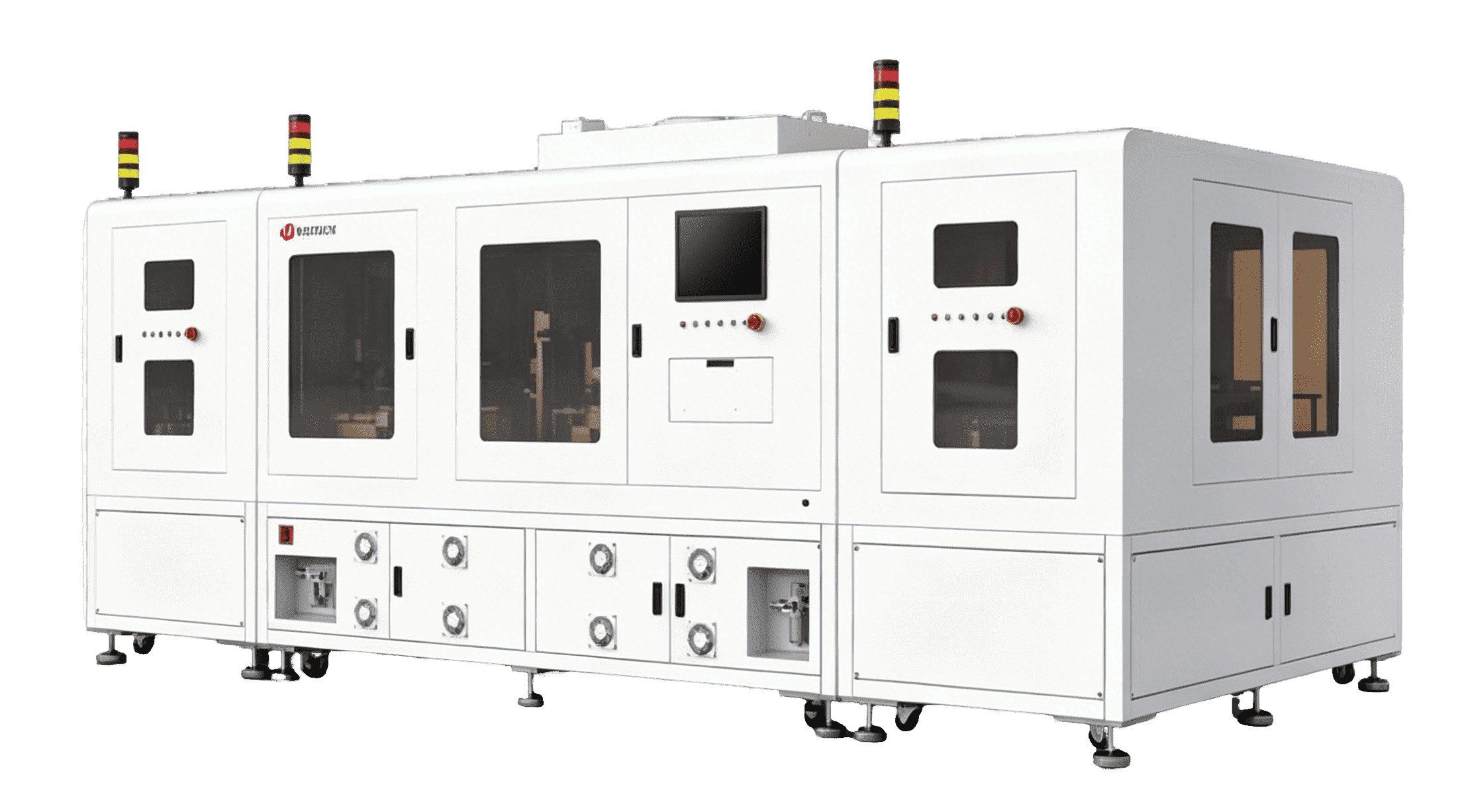
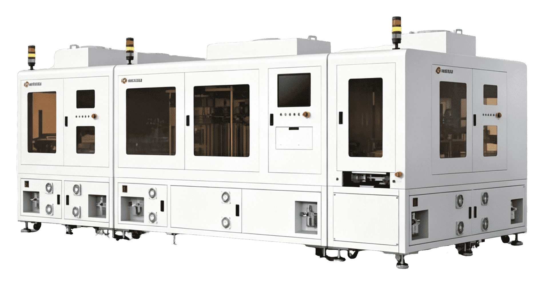
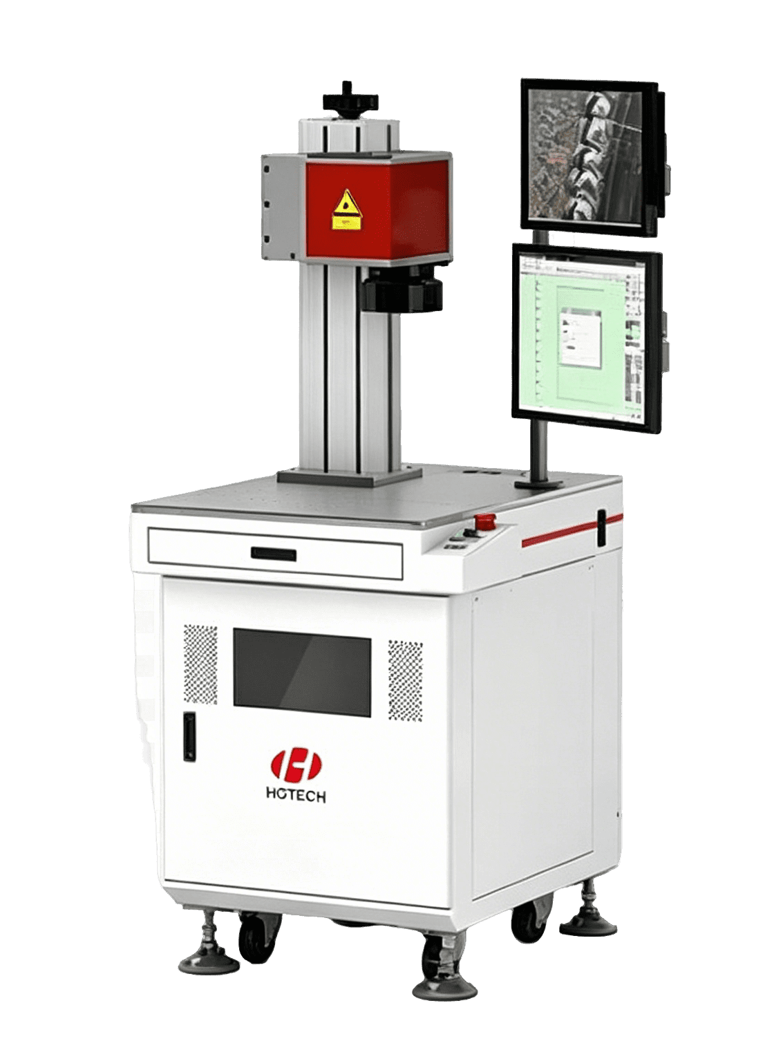
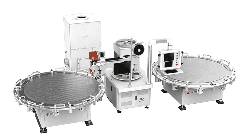
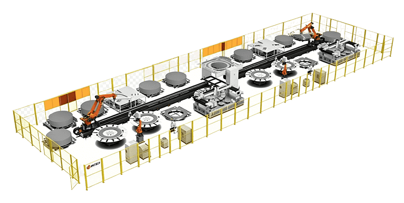
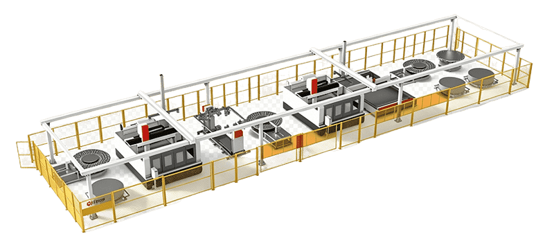
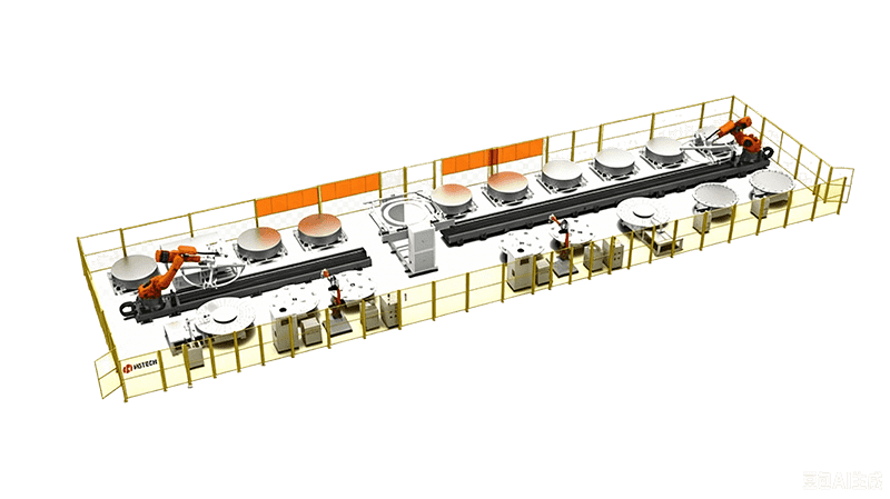
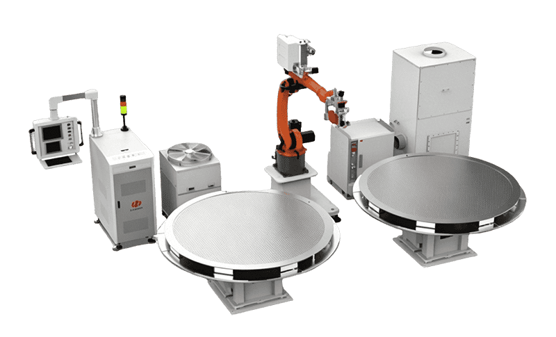
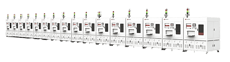
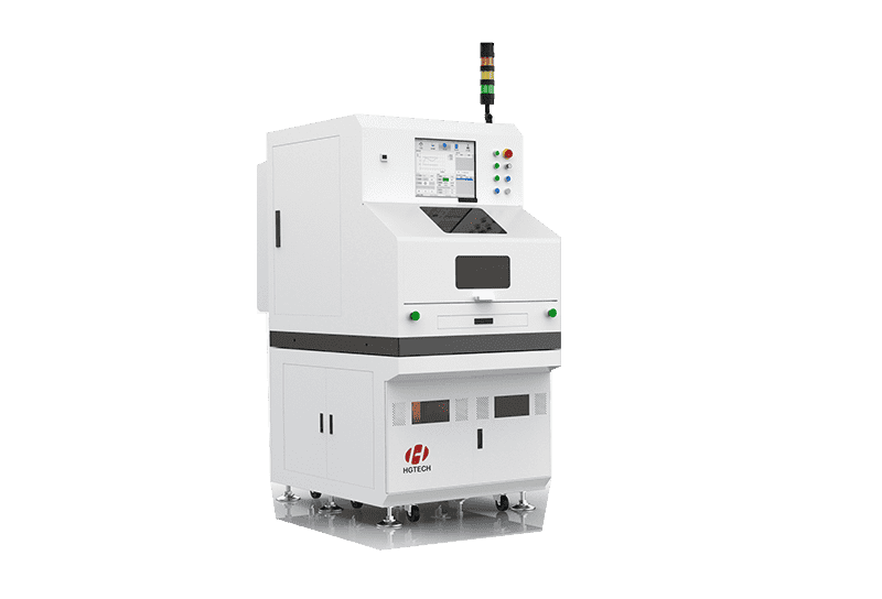
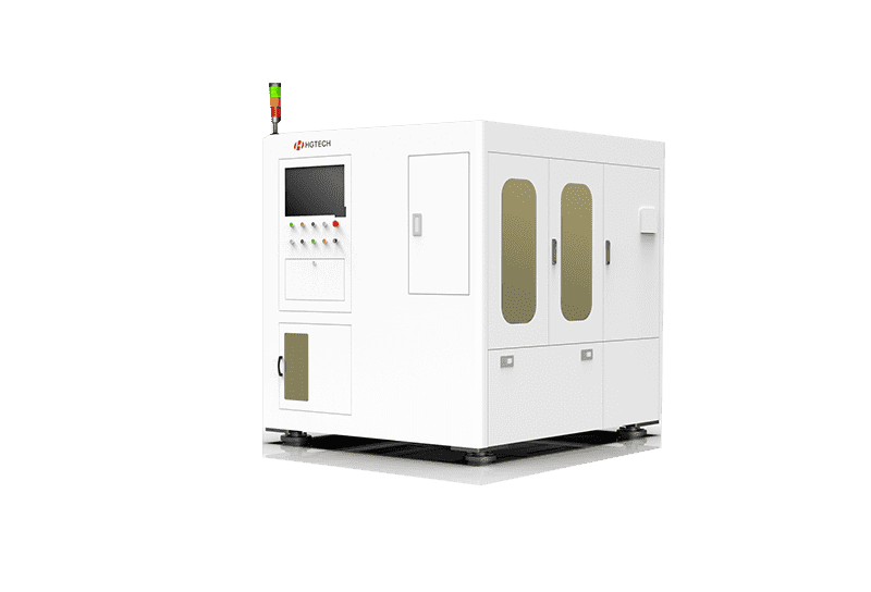
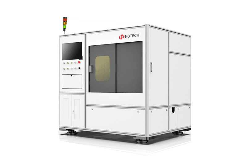
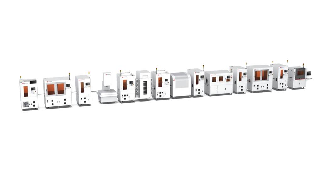
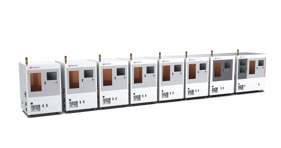
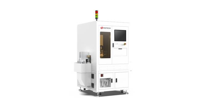
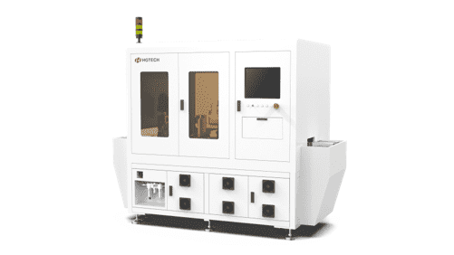
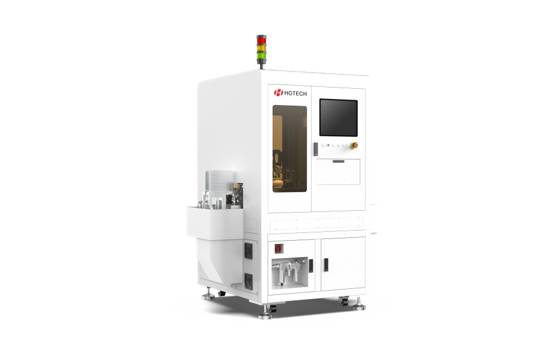
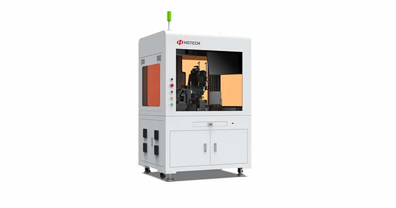
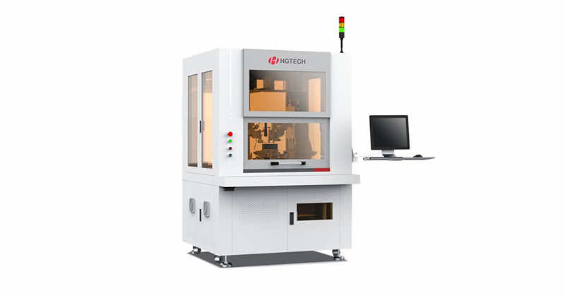
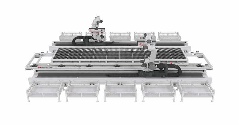
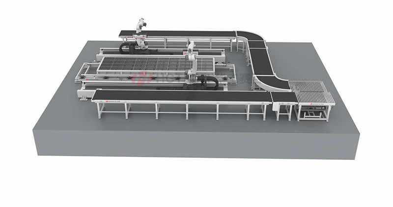
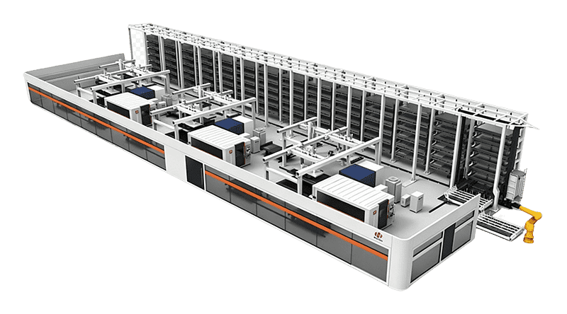


Product advantages:
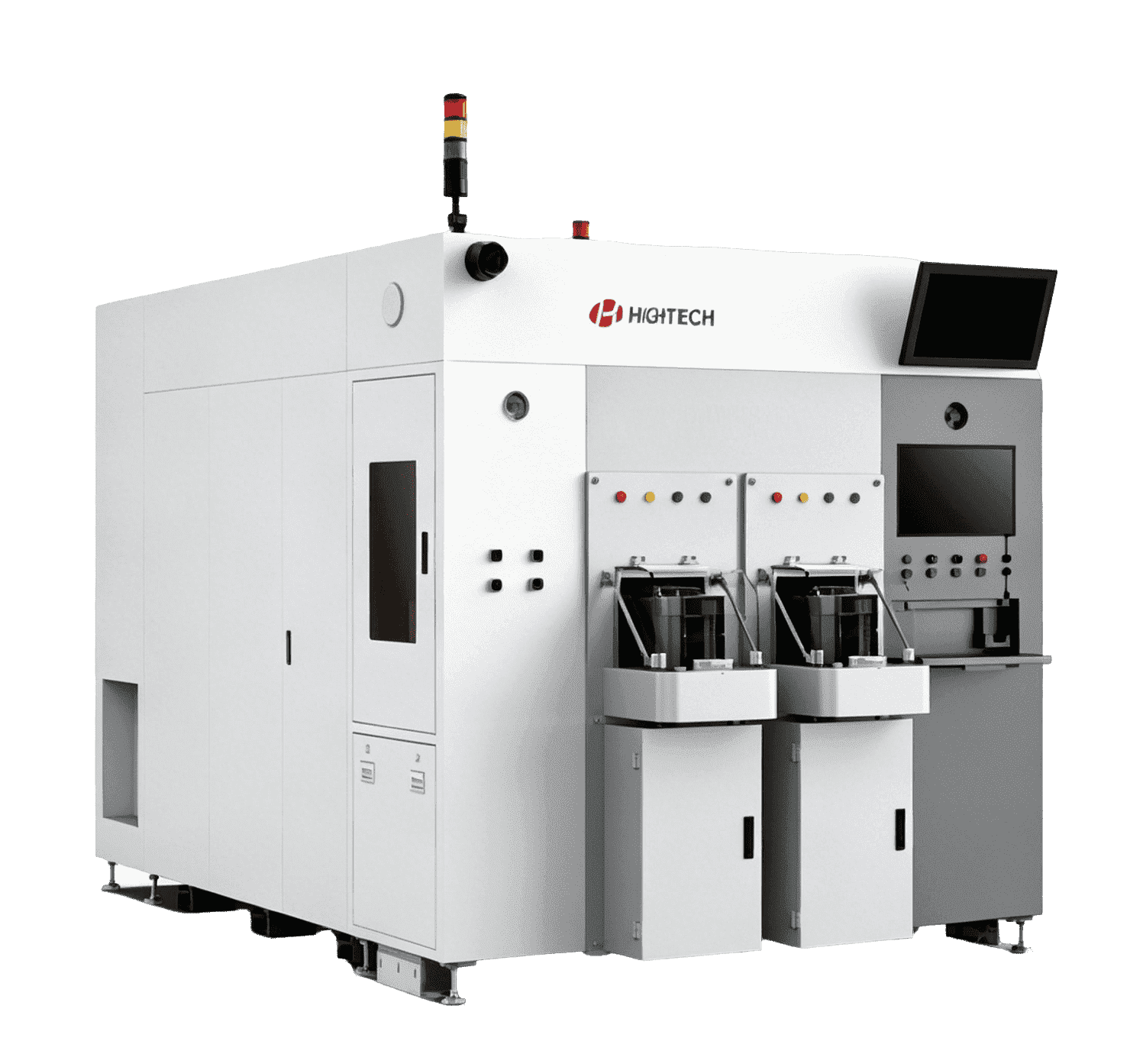
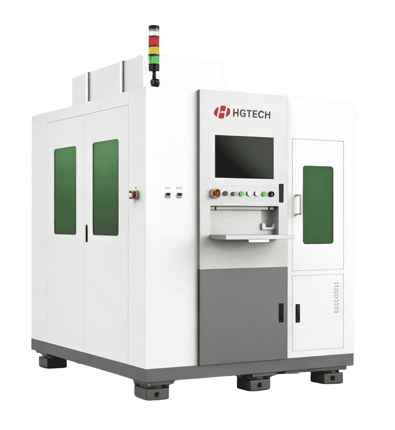
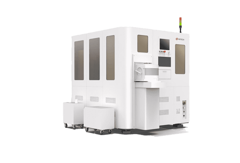
There is no damage on the surface, no cutting seam, and the edge collapse is very small (≤ 2 μ m) , the edge is small (< 3 μ m)
Multi focus modification mode can be adopted to multiply the cutting efficiency
The laser has high average power stability (≤± 3% over 24 hours) and high beam quality (M ² < 1.5)
Sample display:
Schematic diagram of cutting section
8 inch silicon-based wafer, single point layer by layer modification, thickness 730 μ m

Upper surface (chip structure surface)
8 inch silicon-based wafer, single point layer by layer modification, thickness 730 μ m

Lower surface: chip structure surface
8 inch silicon-based wafer, single point layer by layer modification, thickness 730 μ m