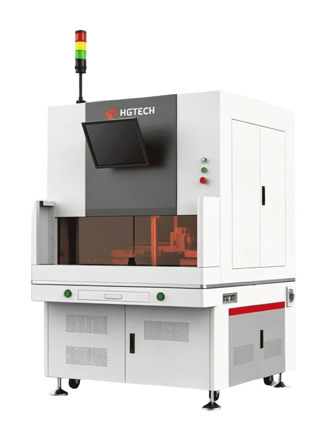
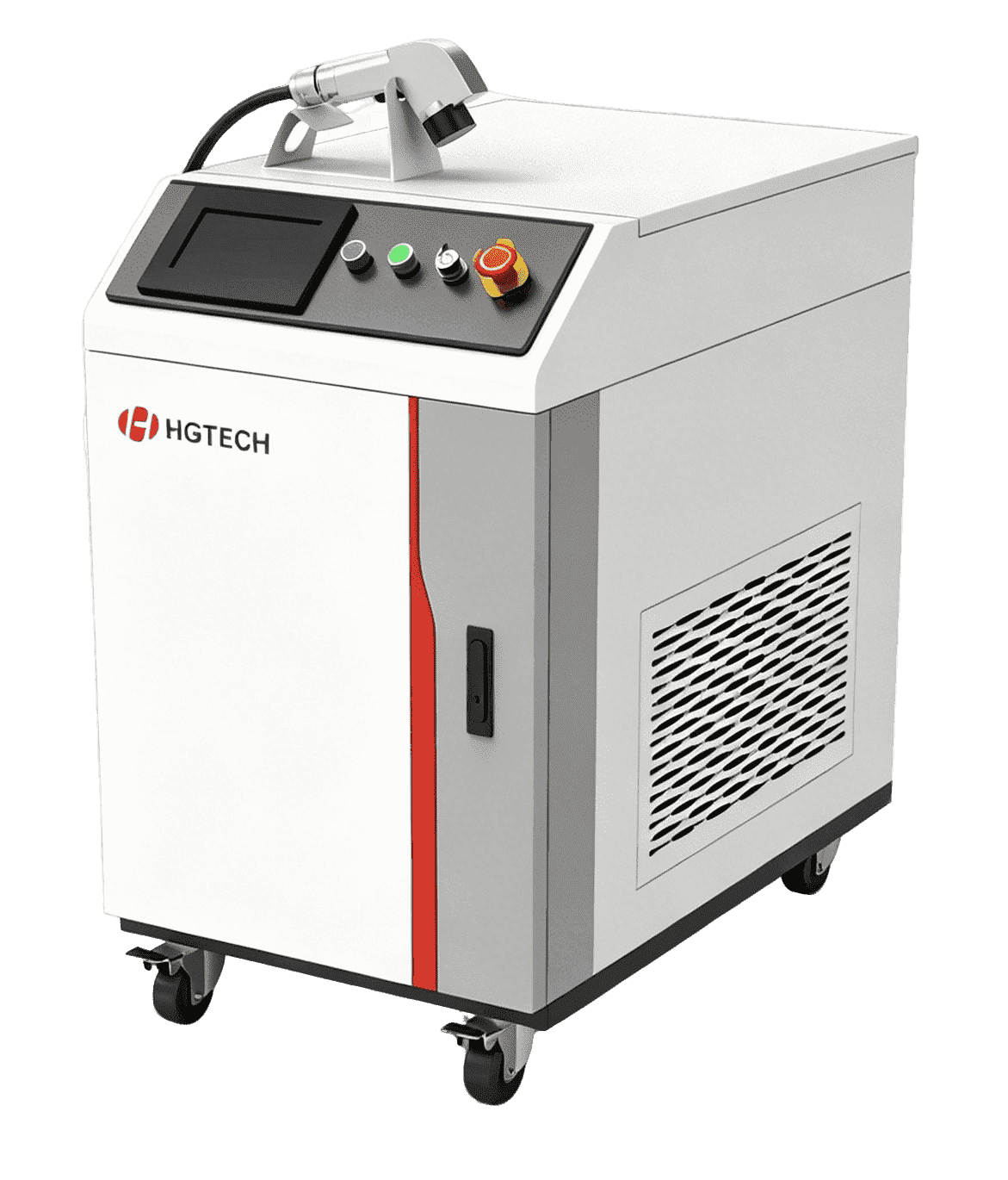
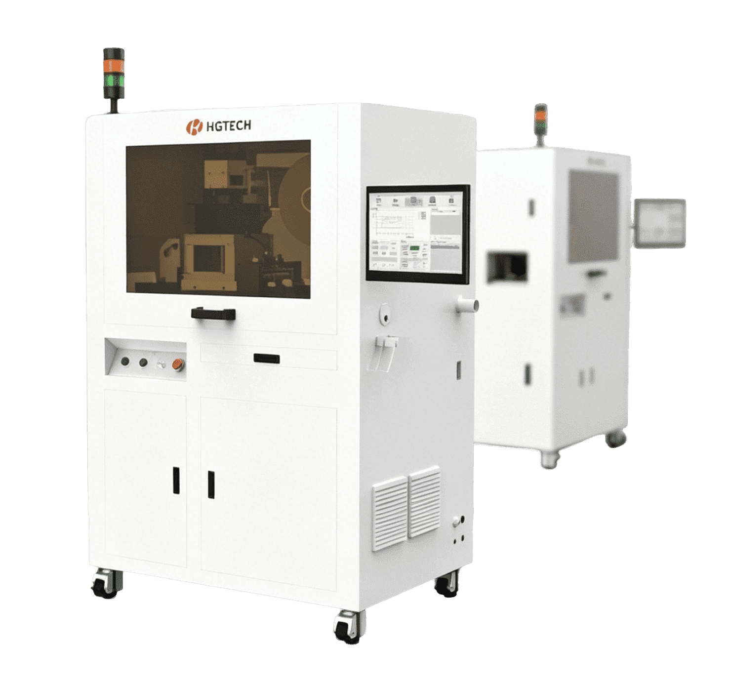
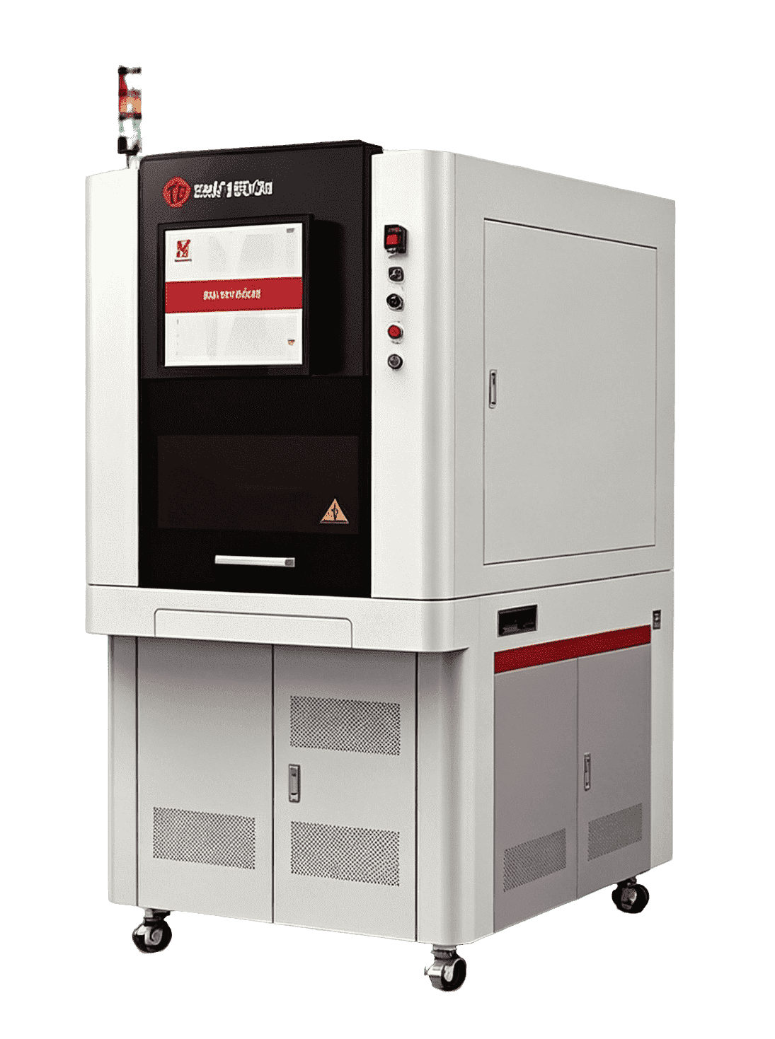
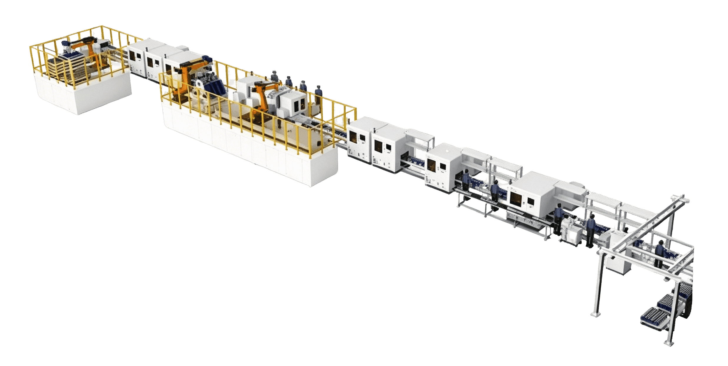
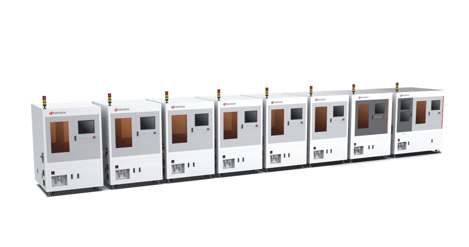
Wafer Thickness Measuring Series
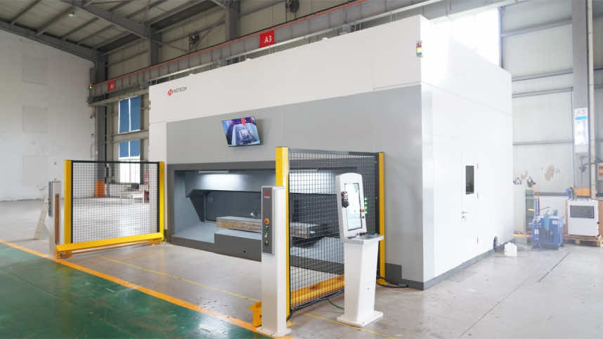
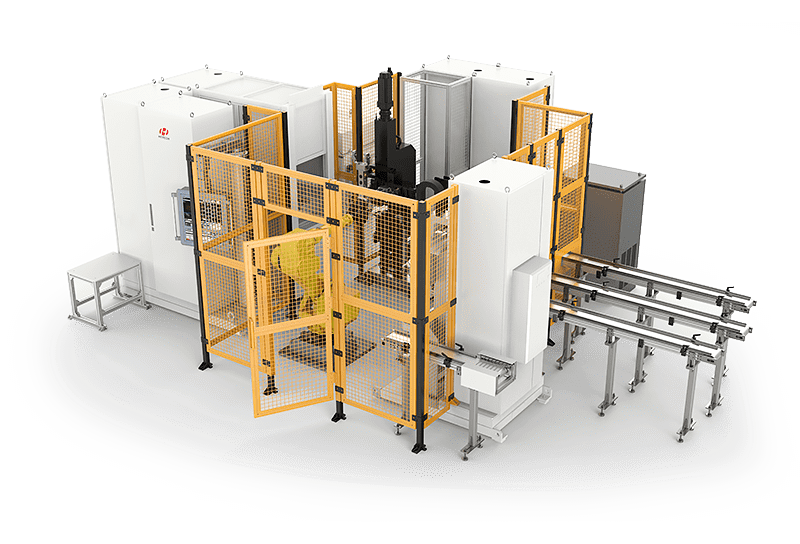
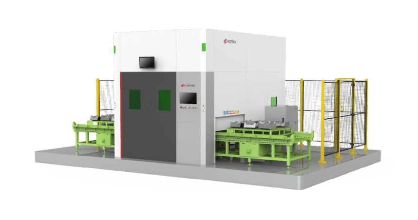
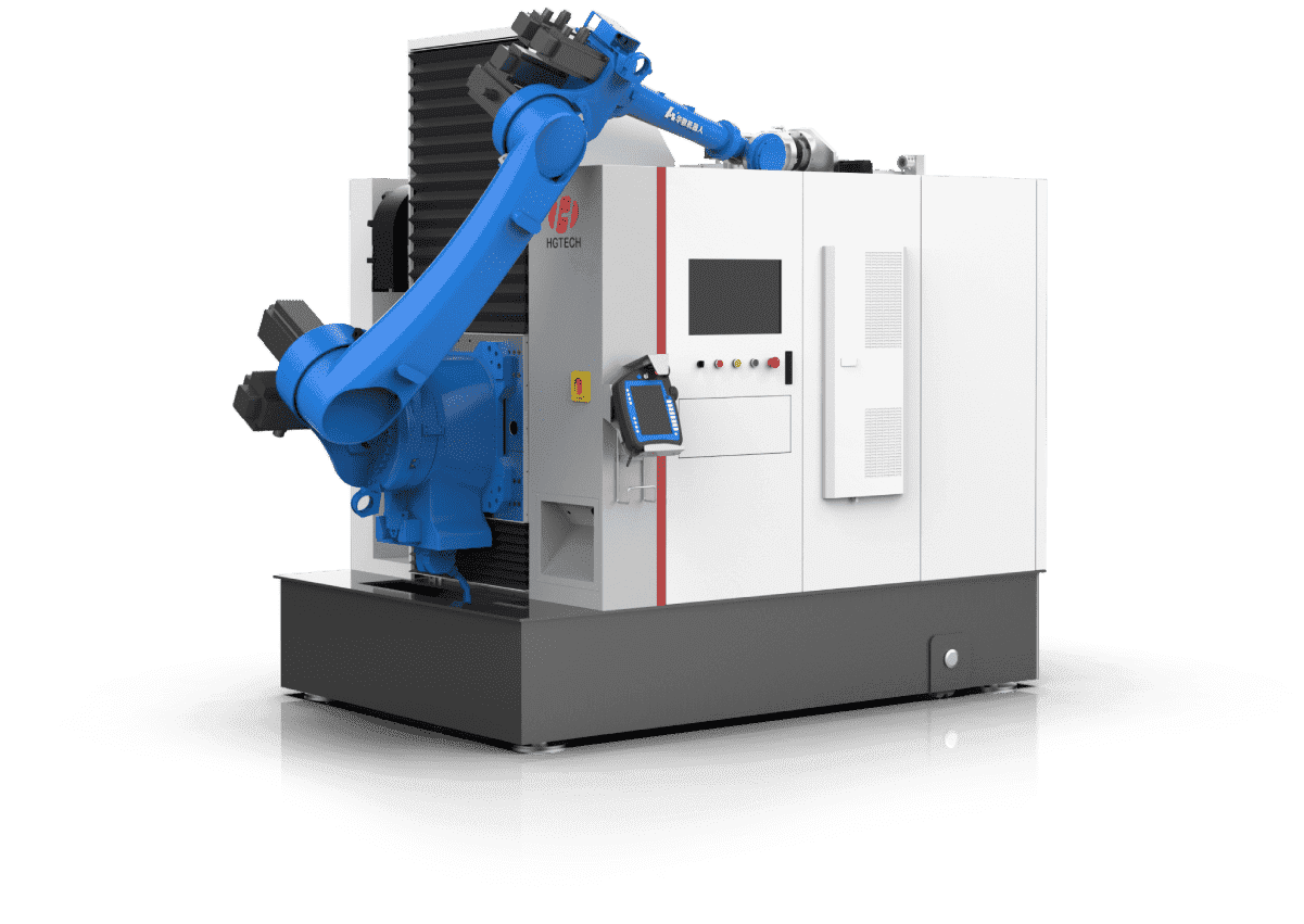
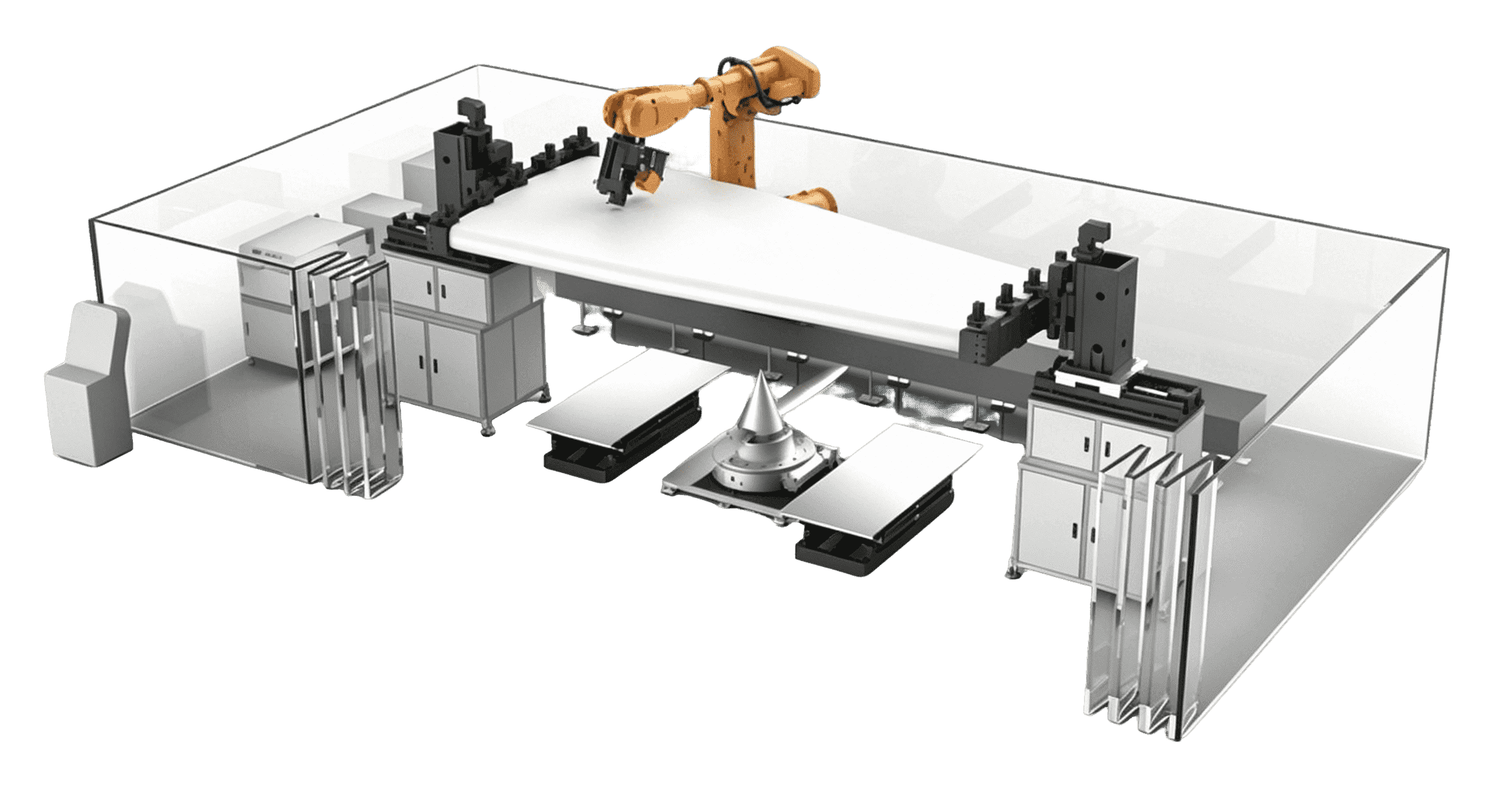
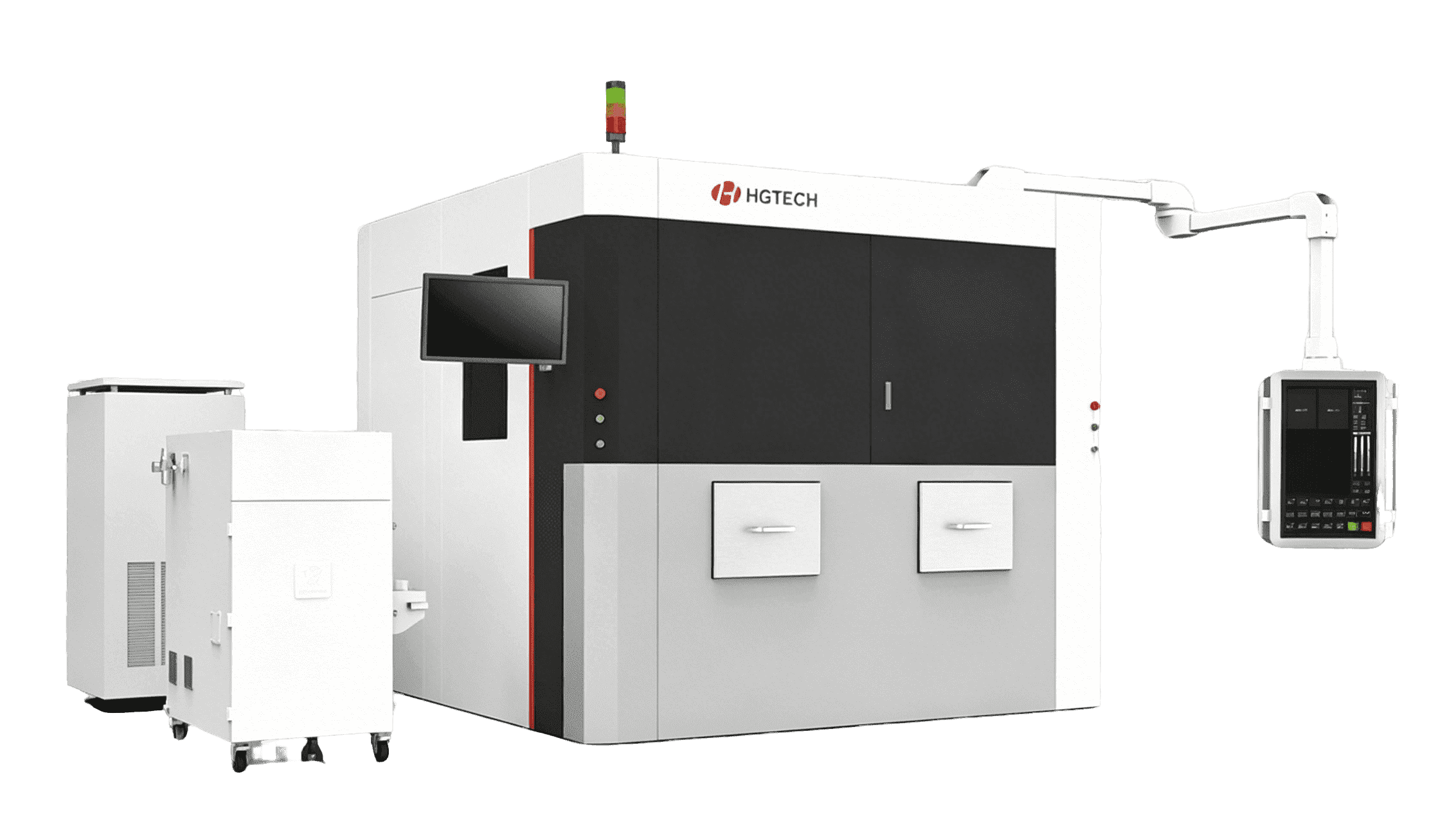
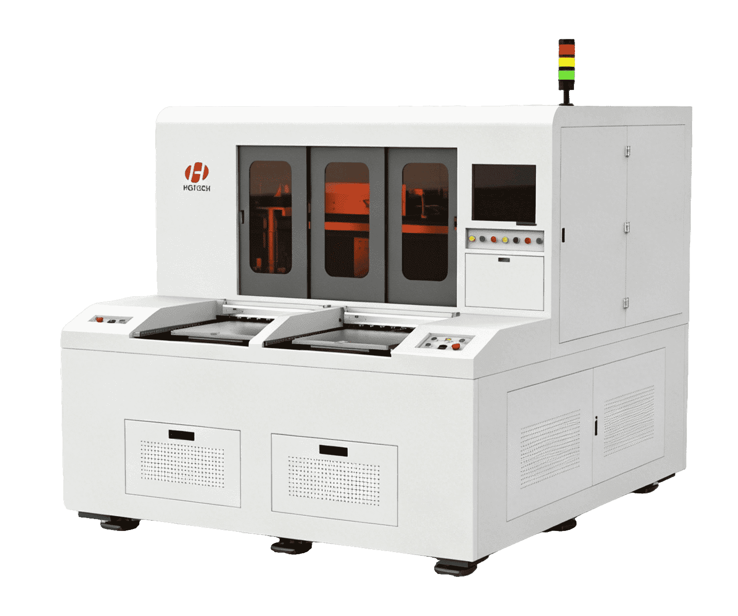
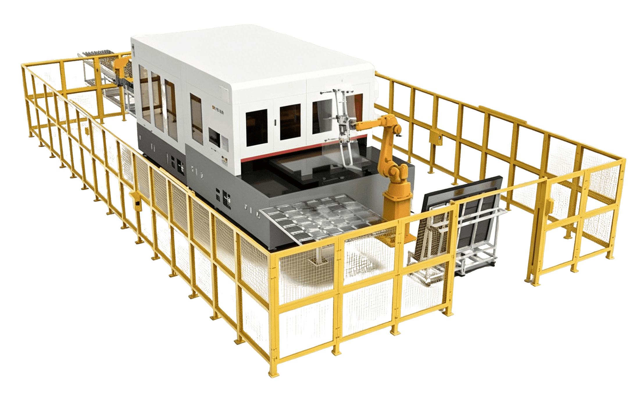
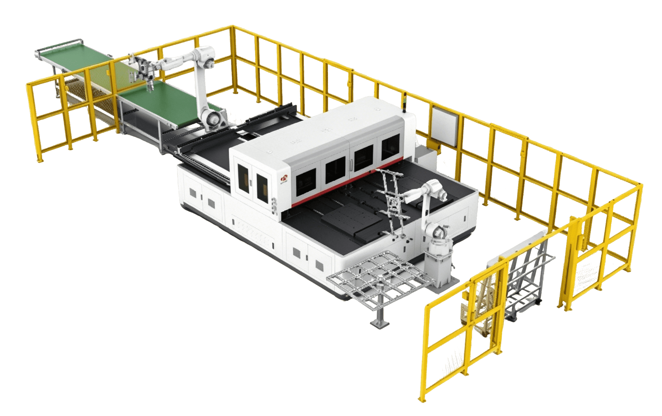
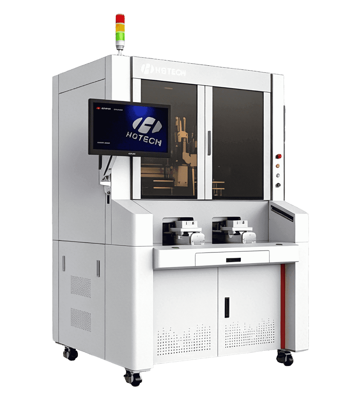
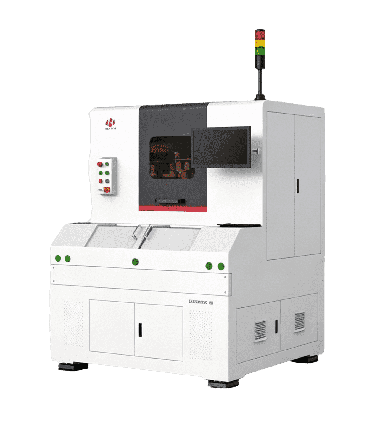
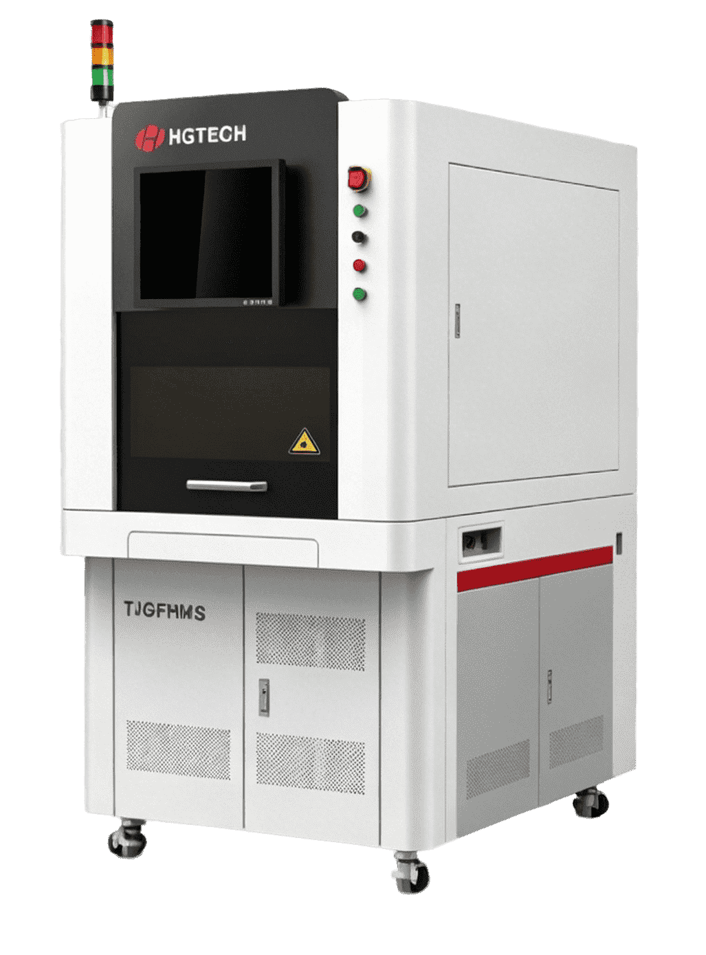
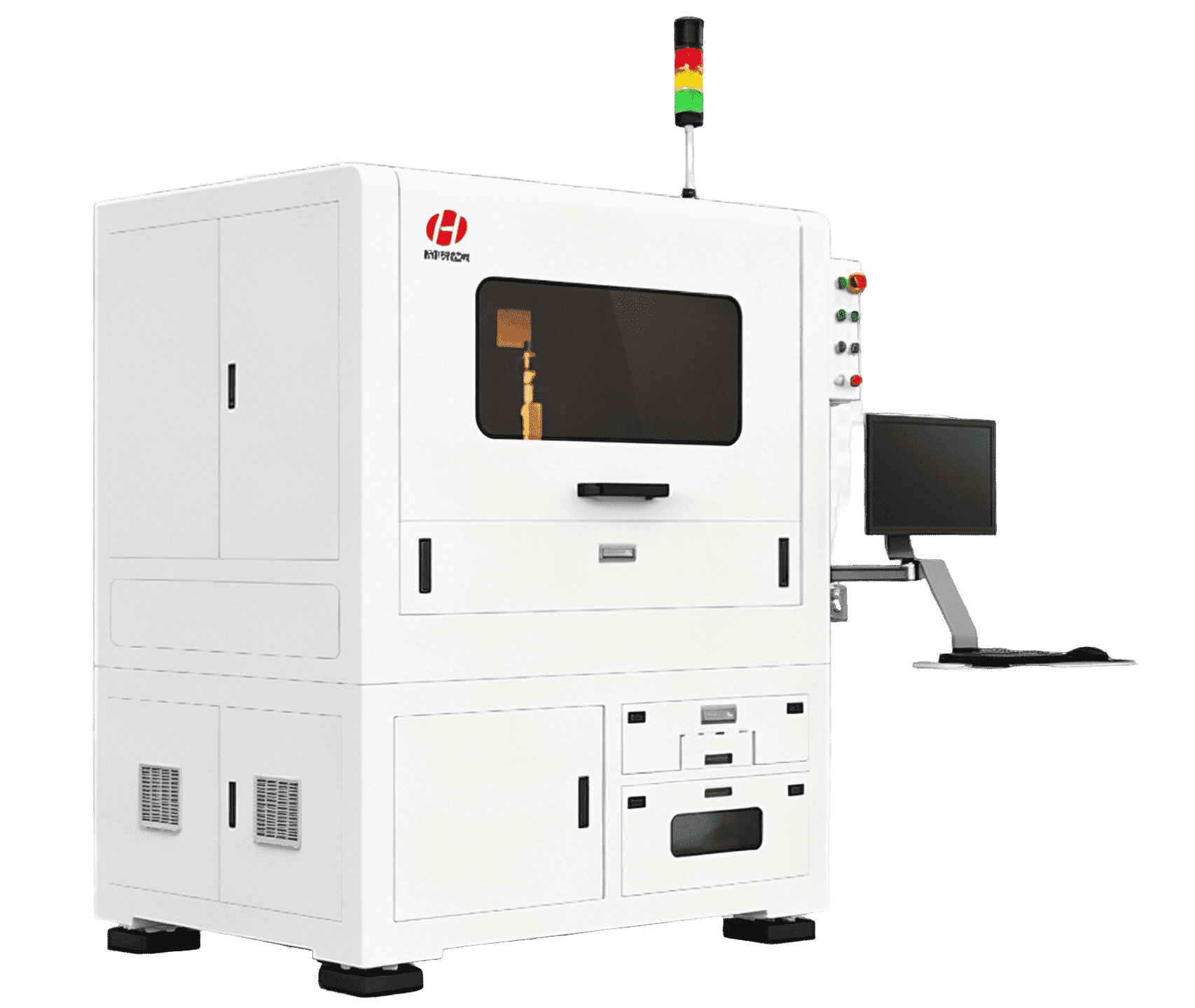
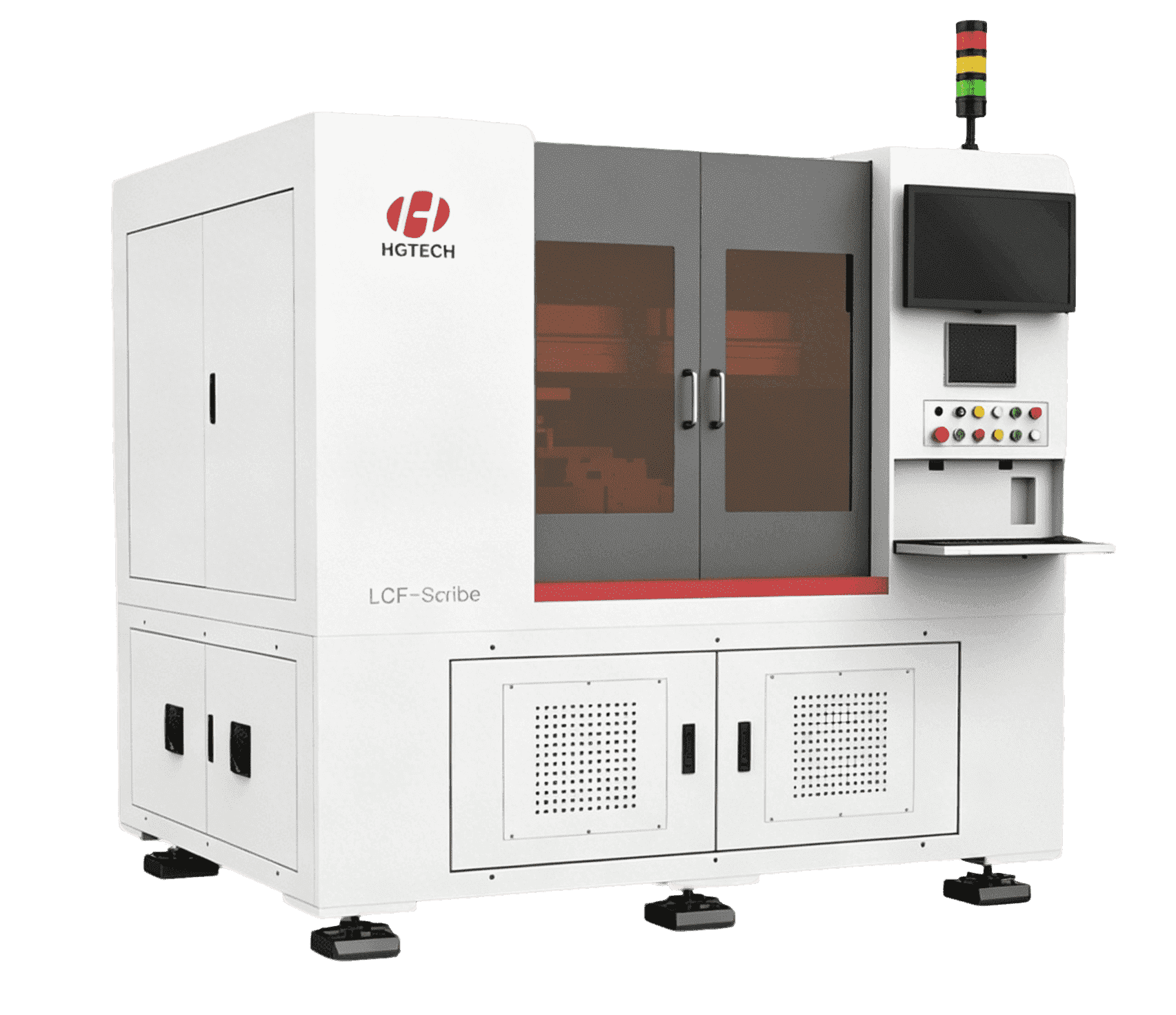
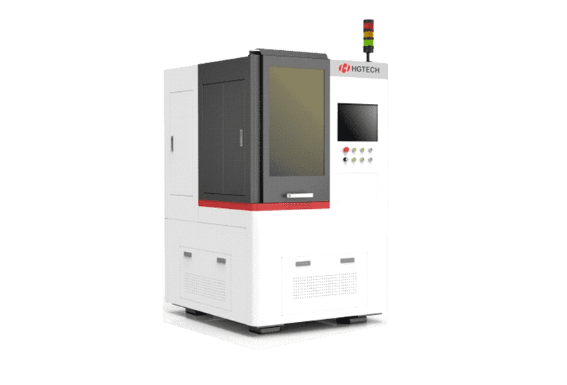
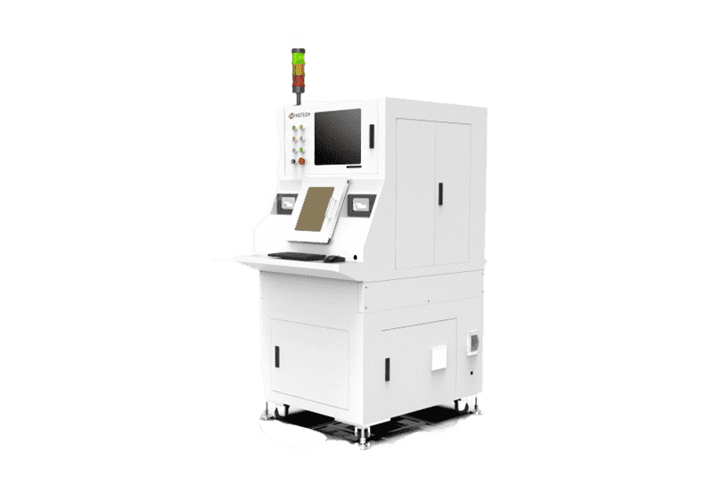
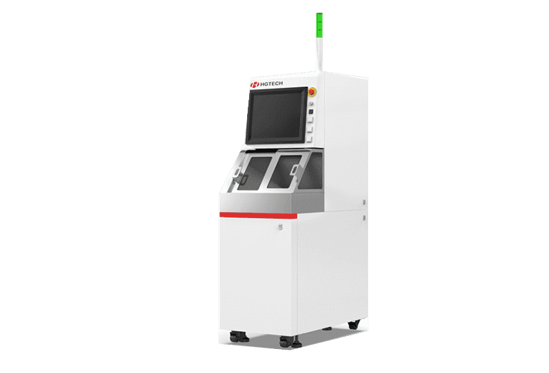
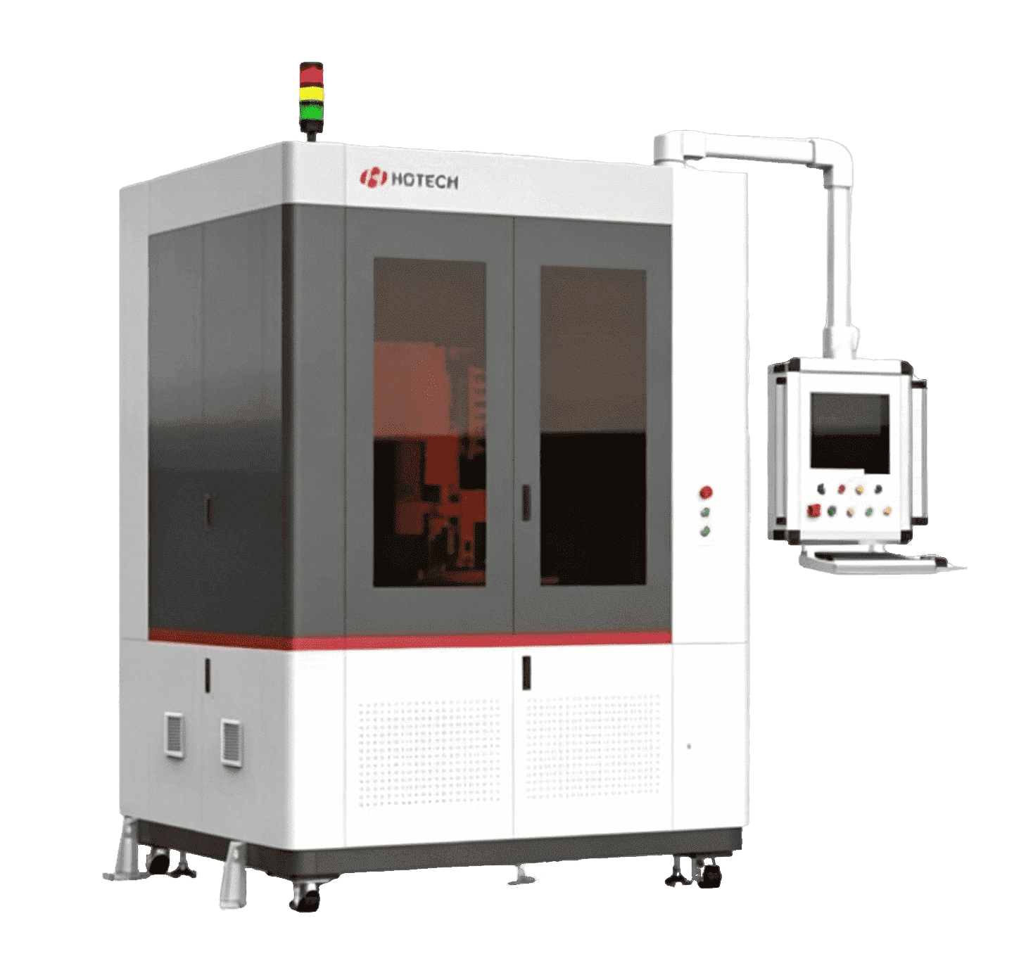
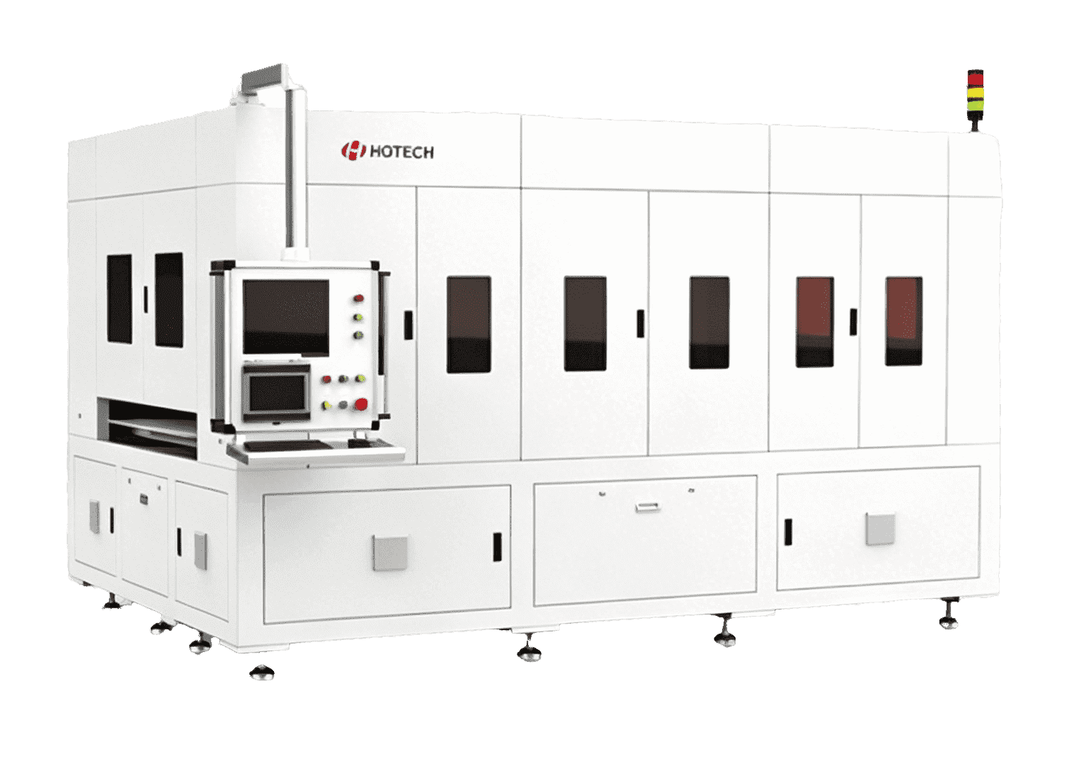
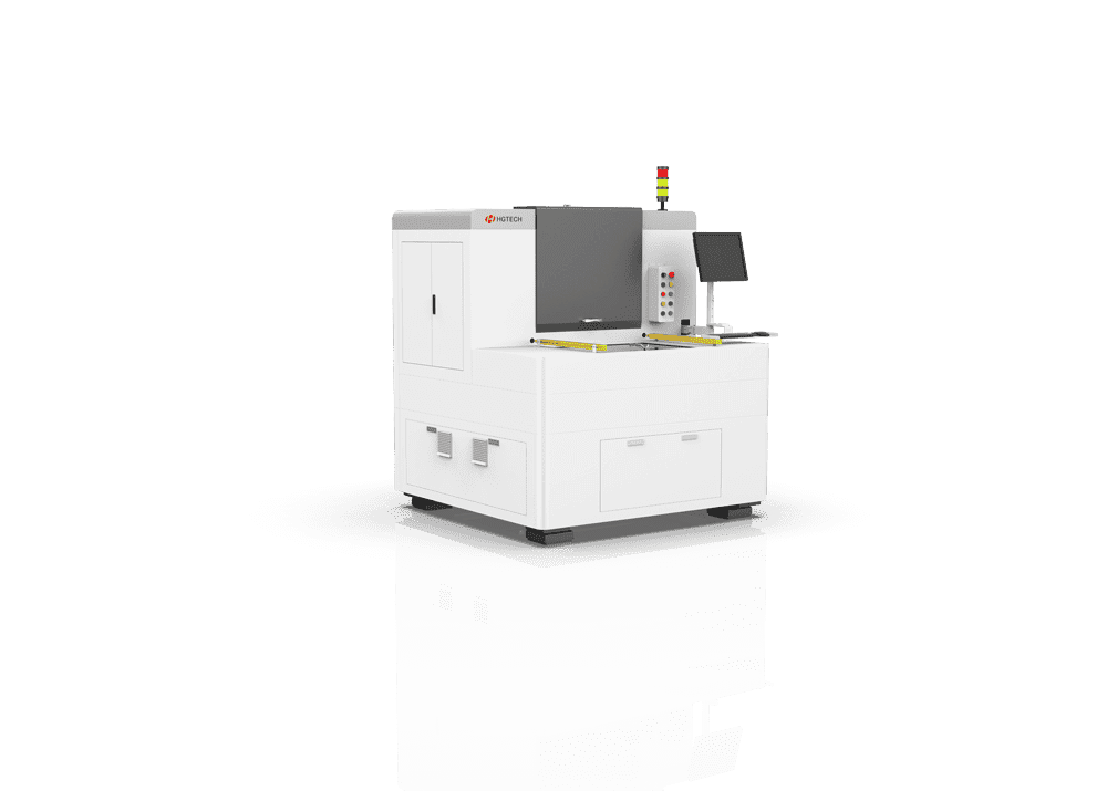
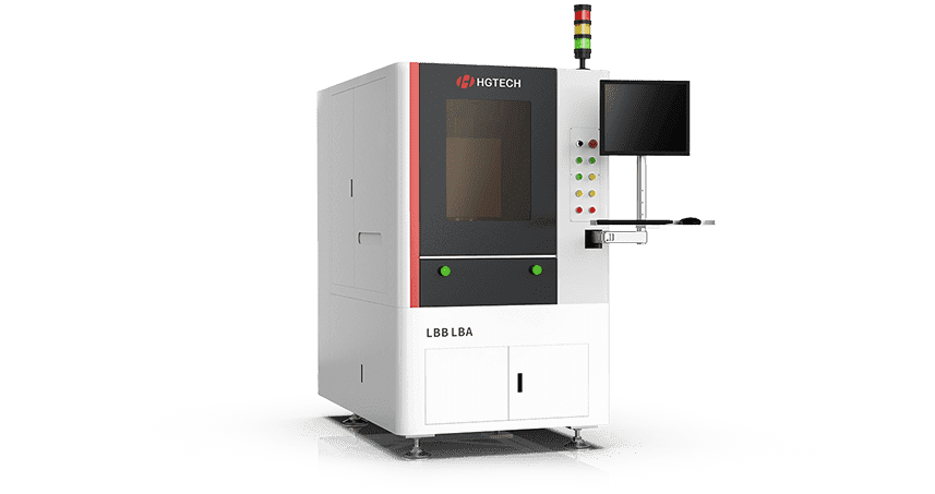
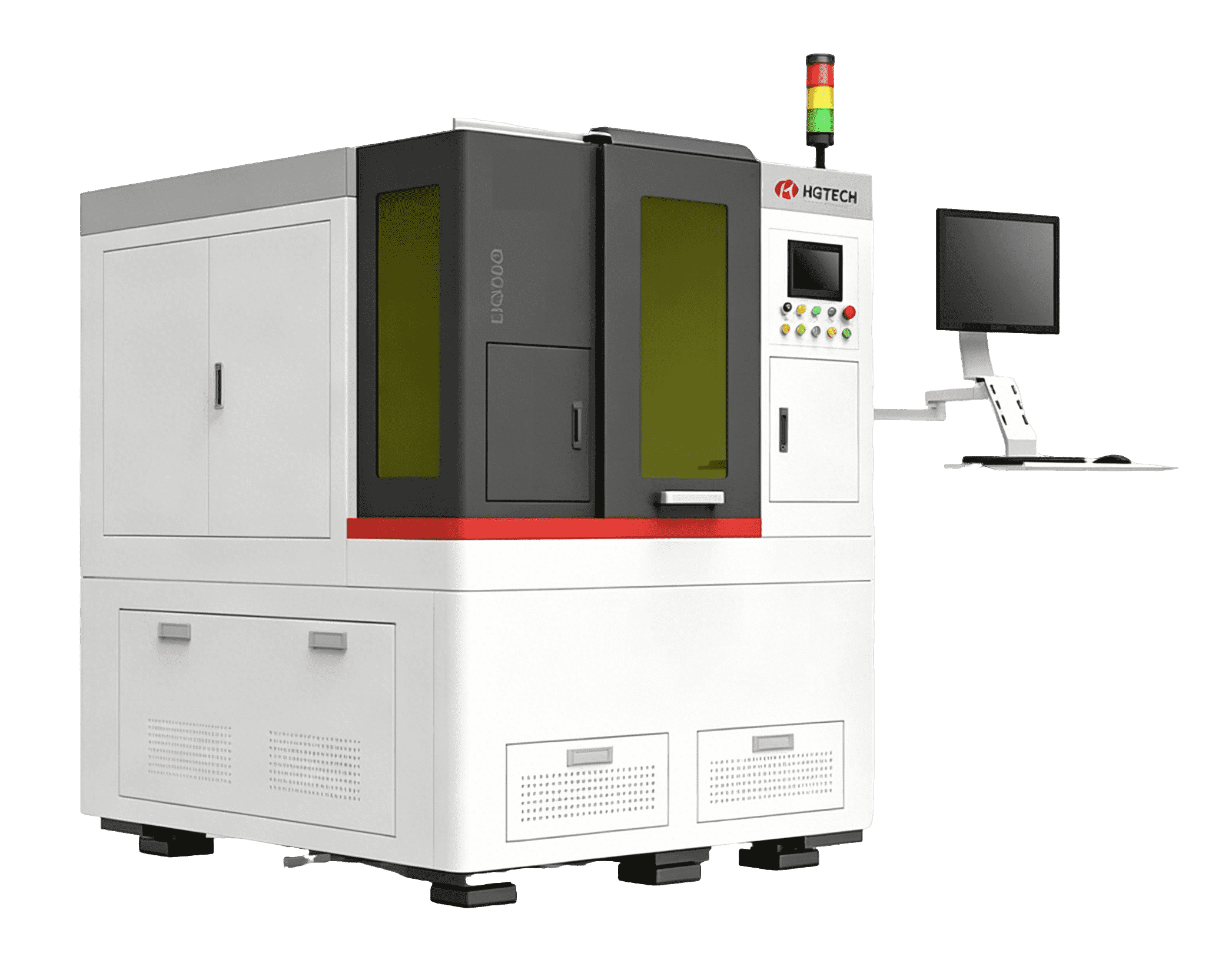
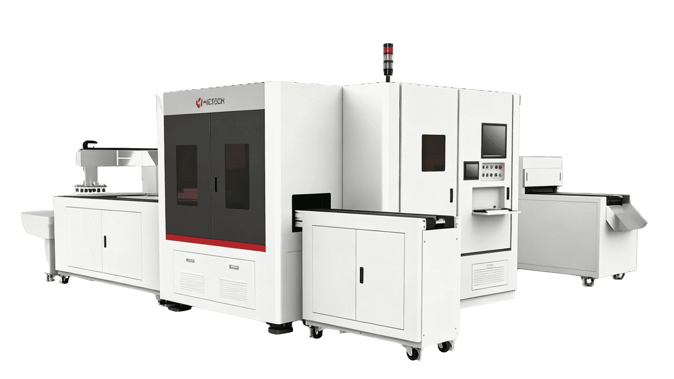
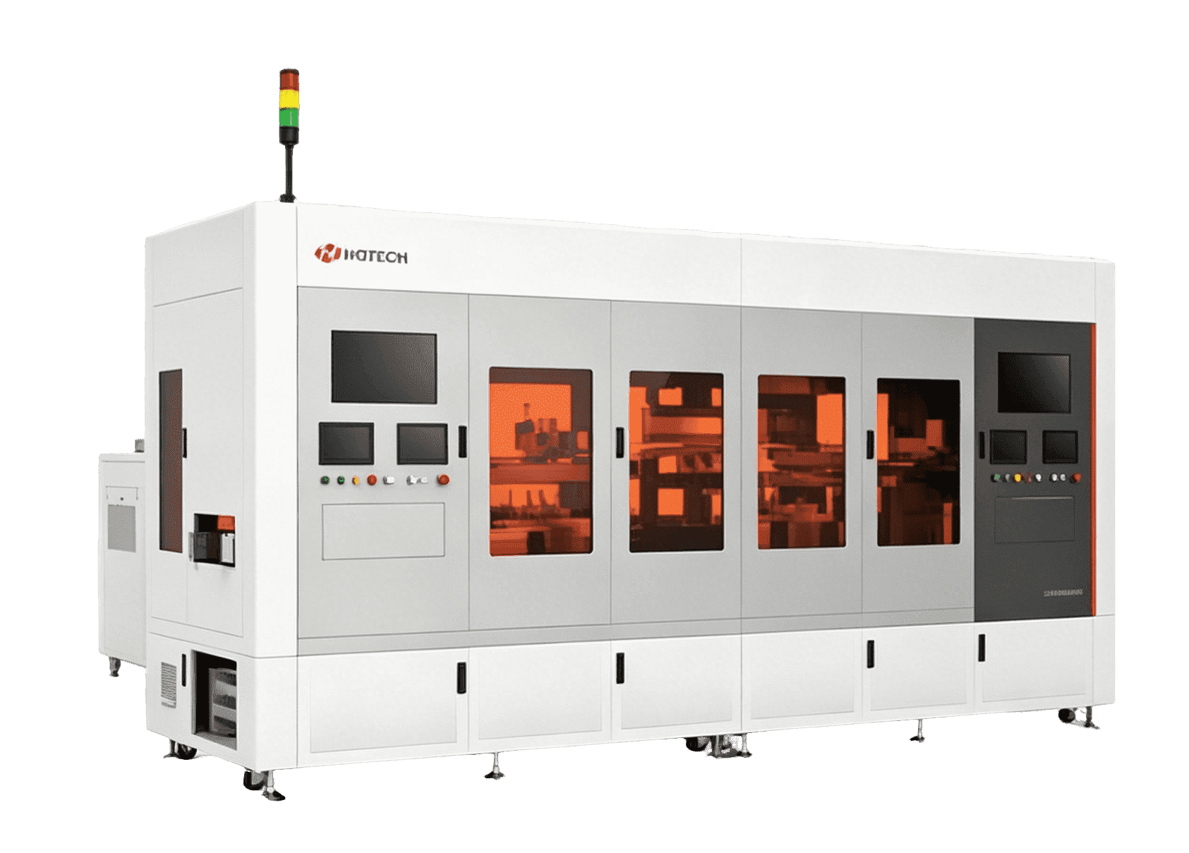
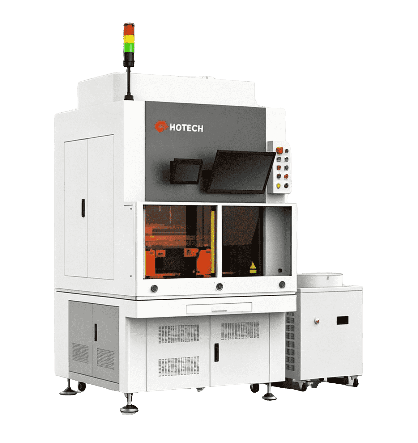
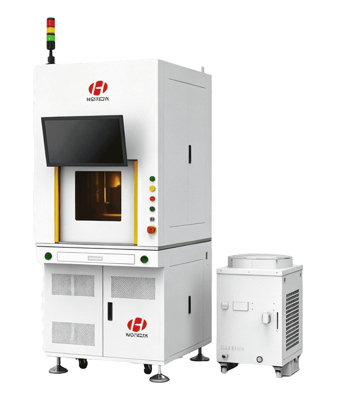
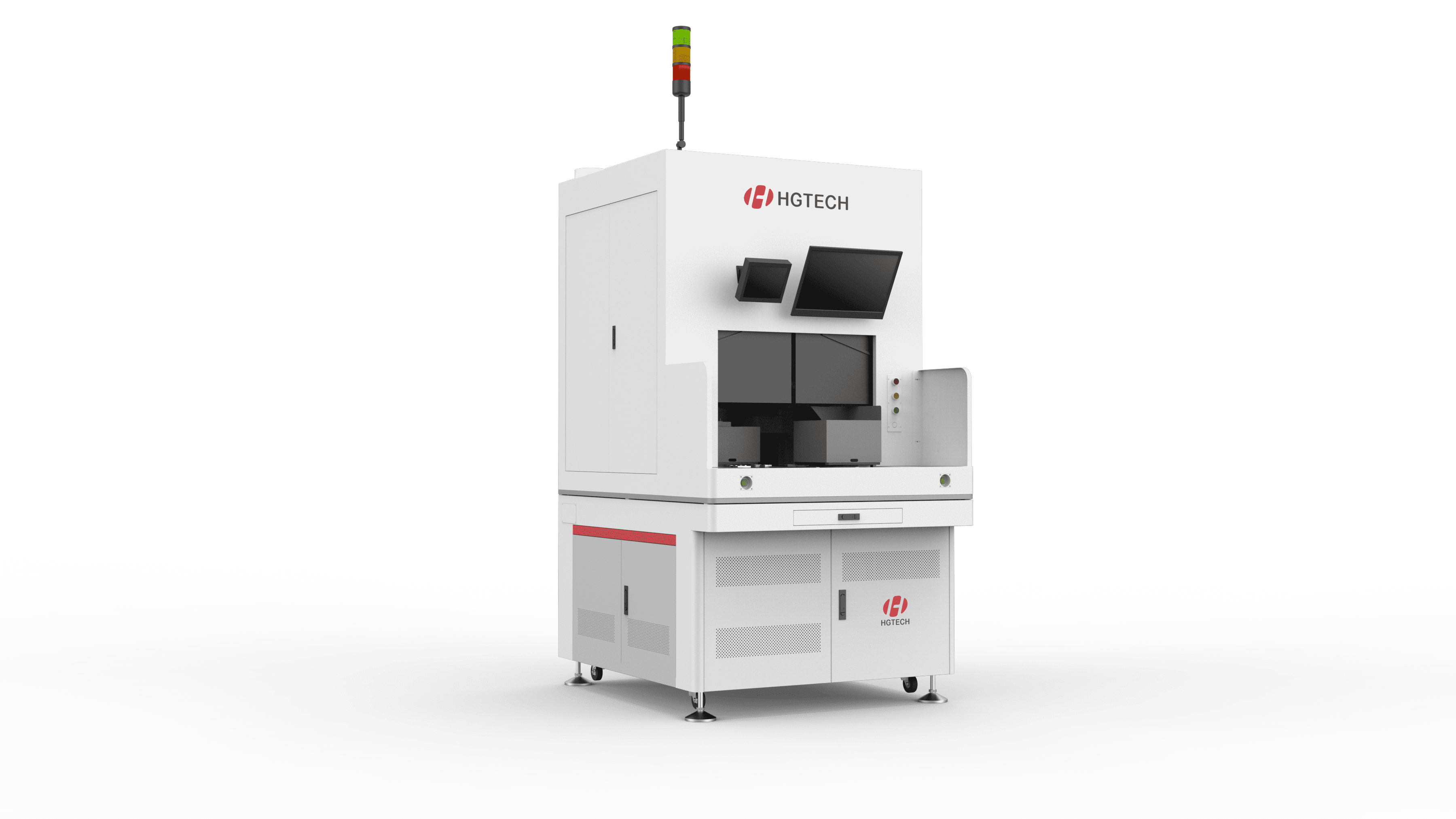
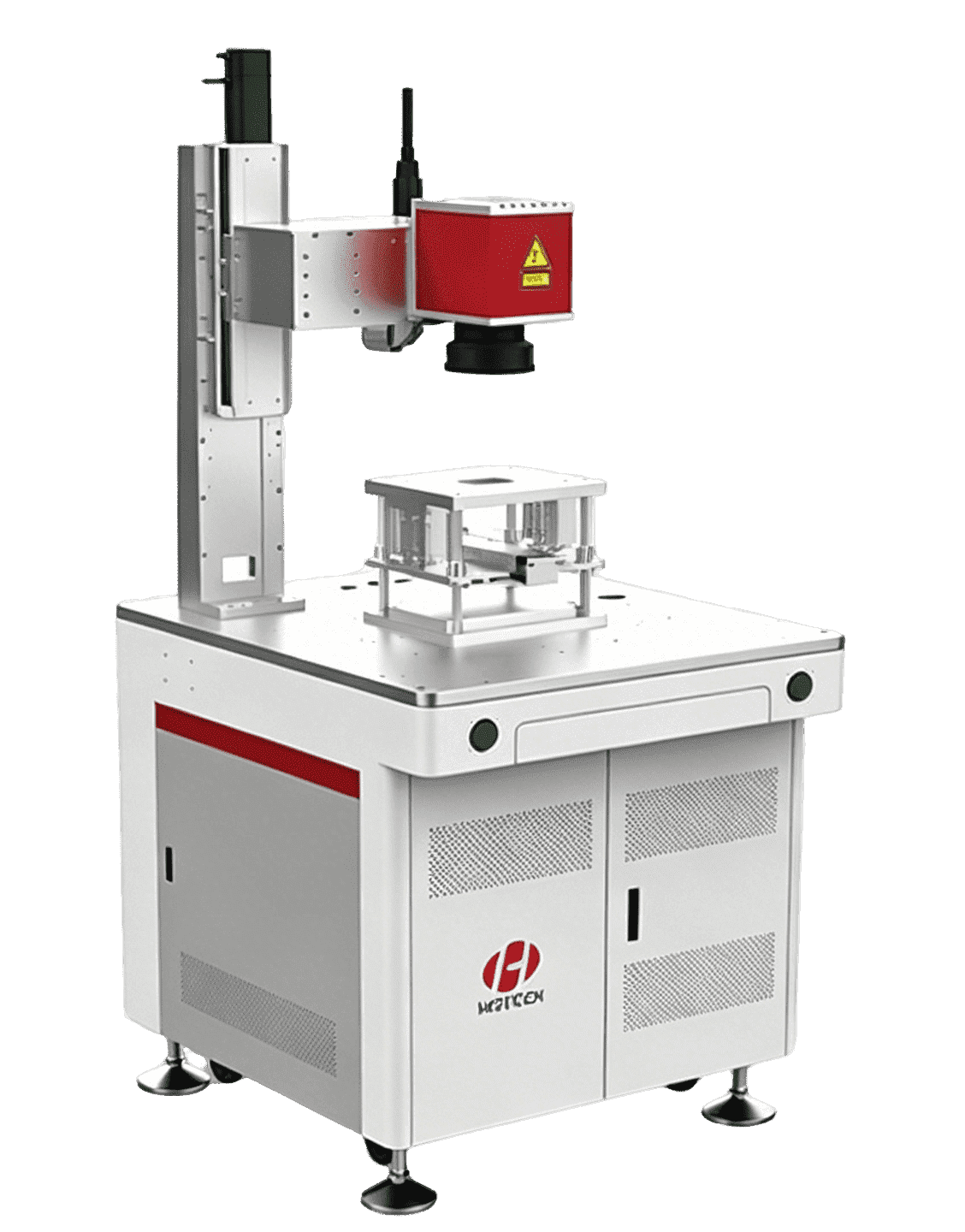
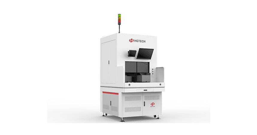
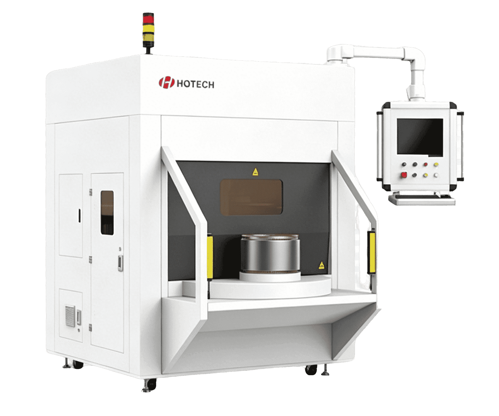
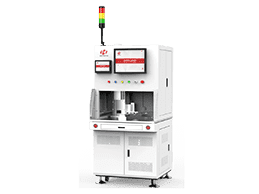
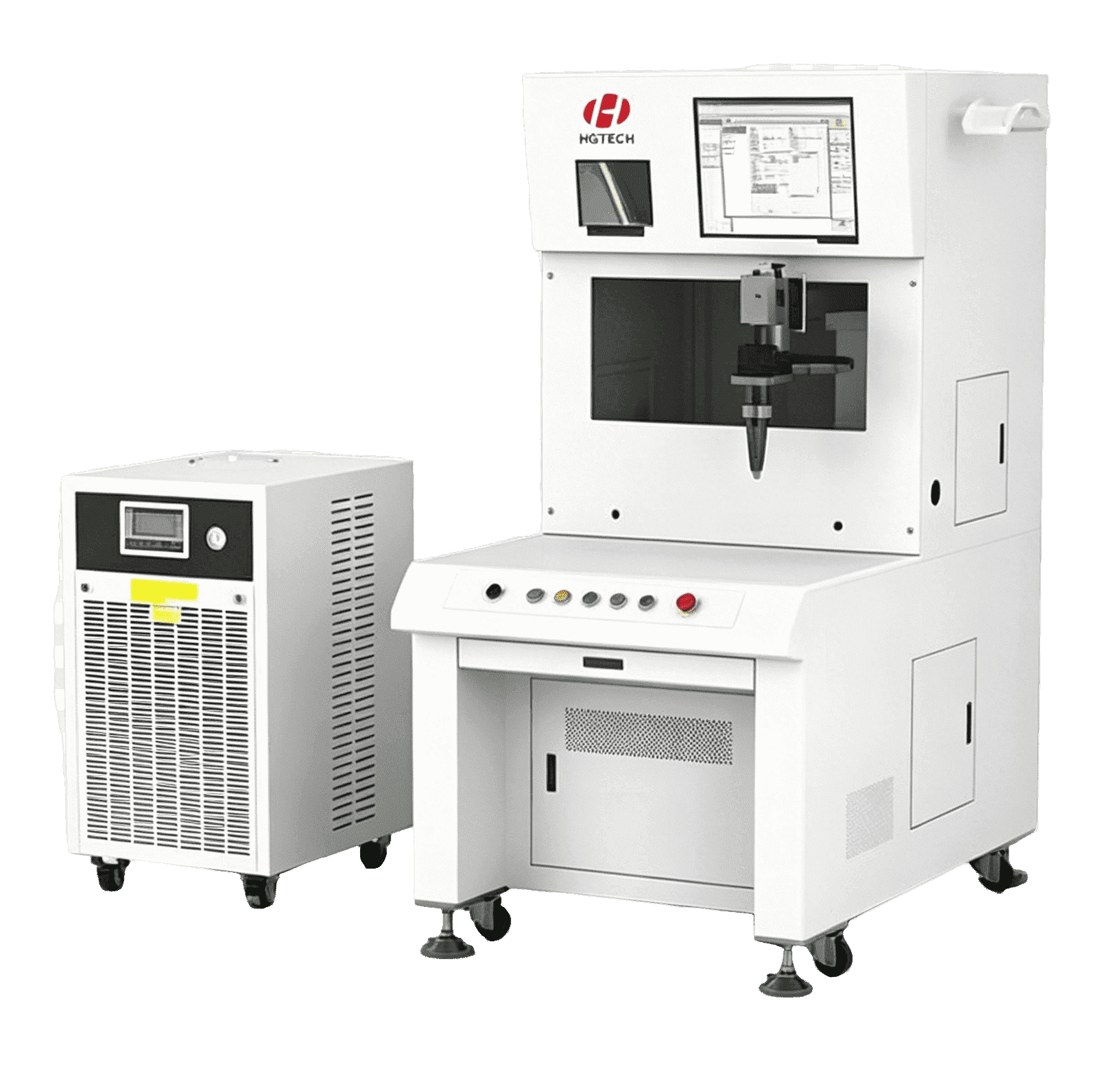
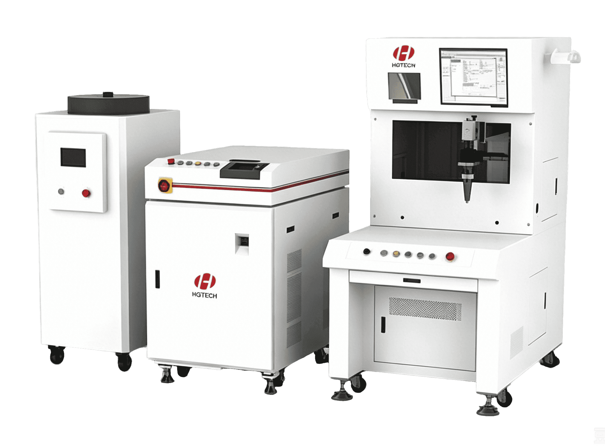
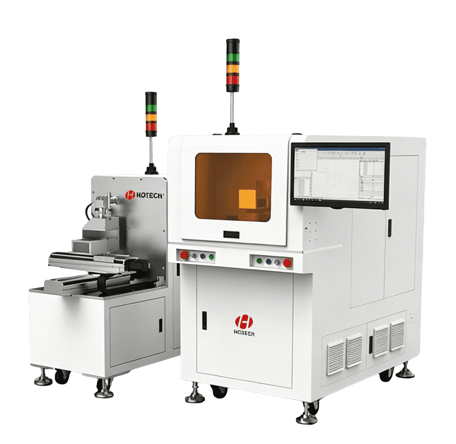
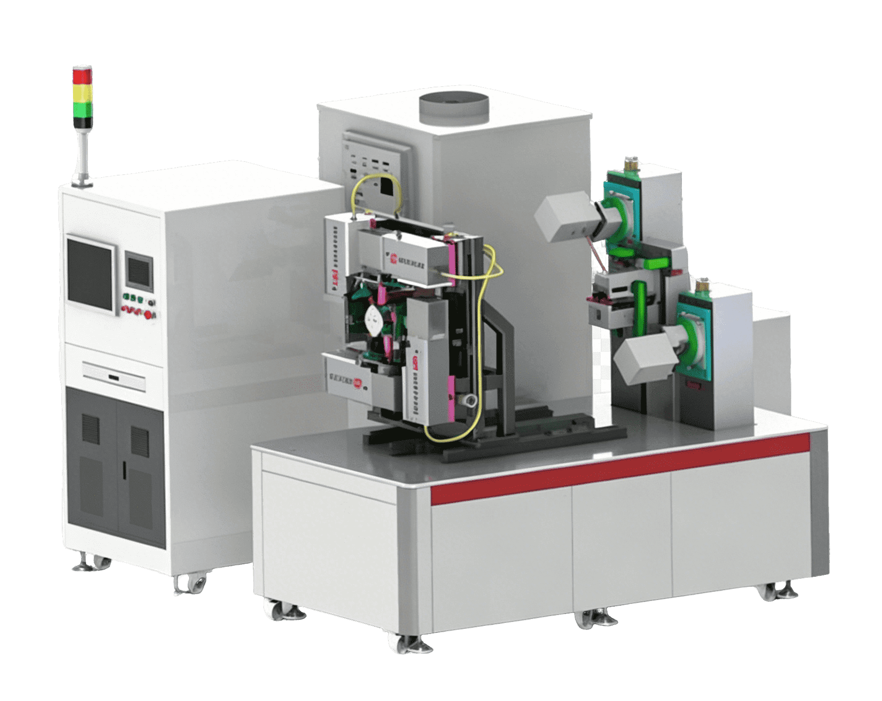
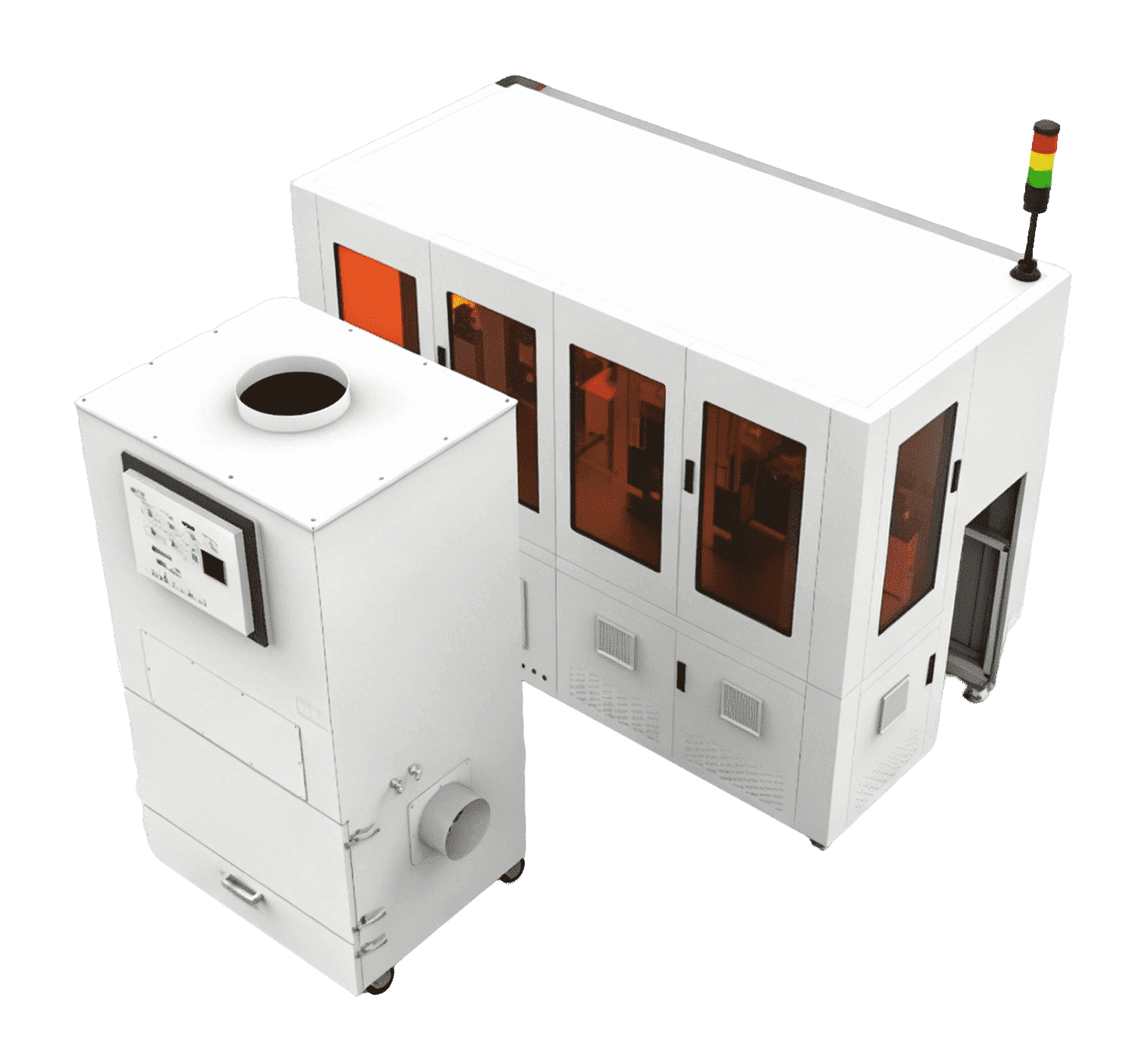
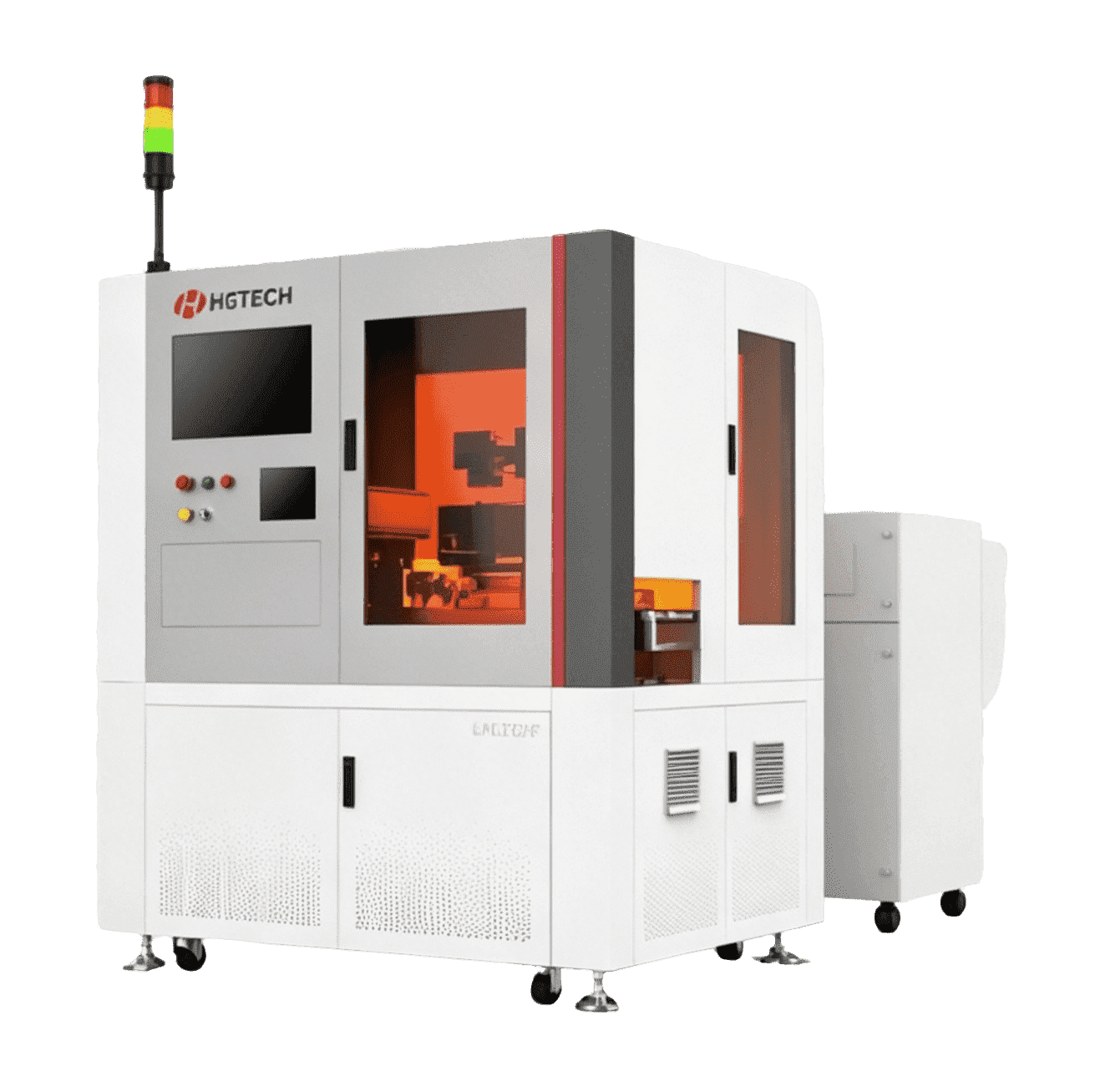
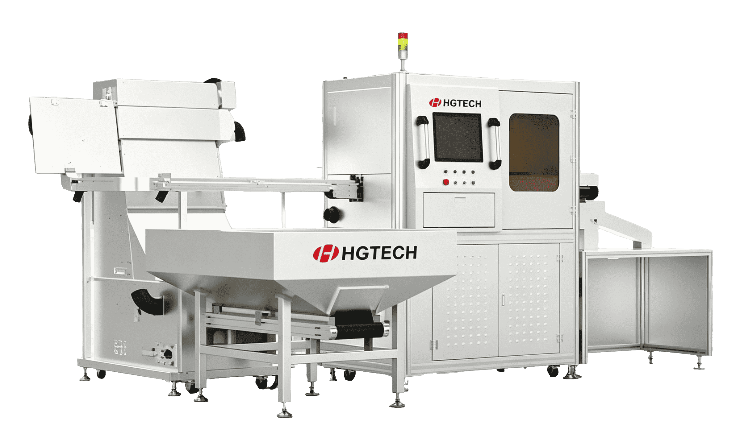
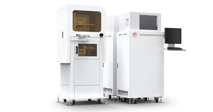
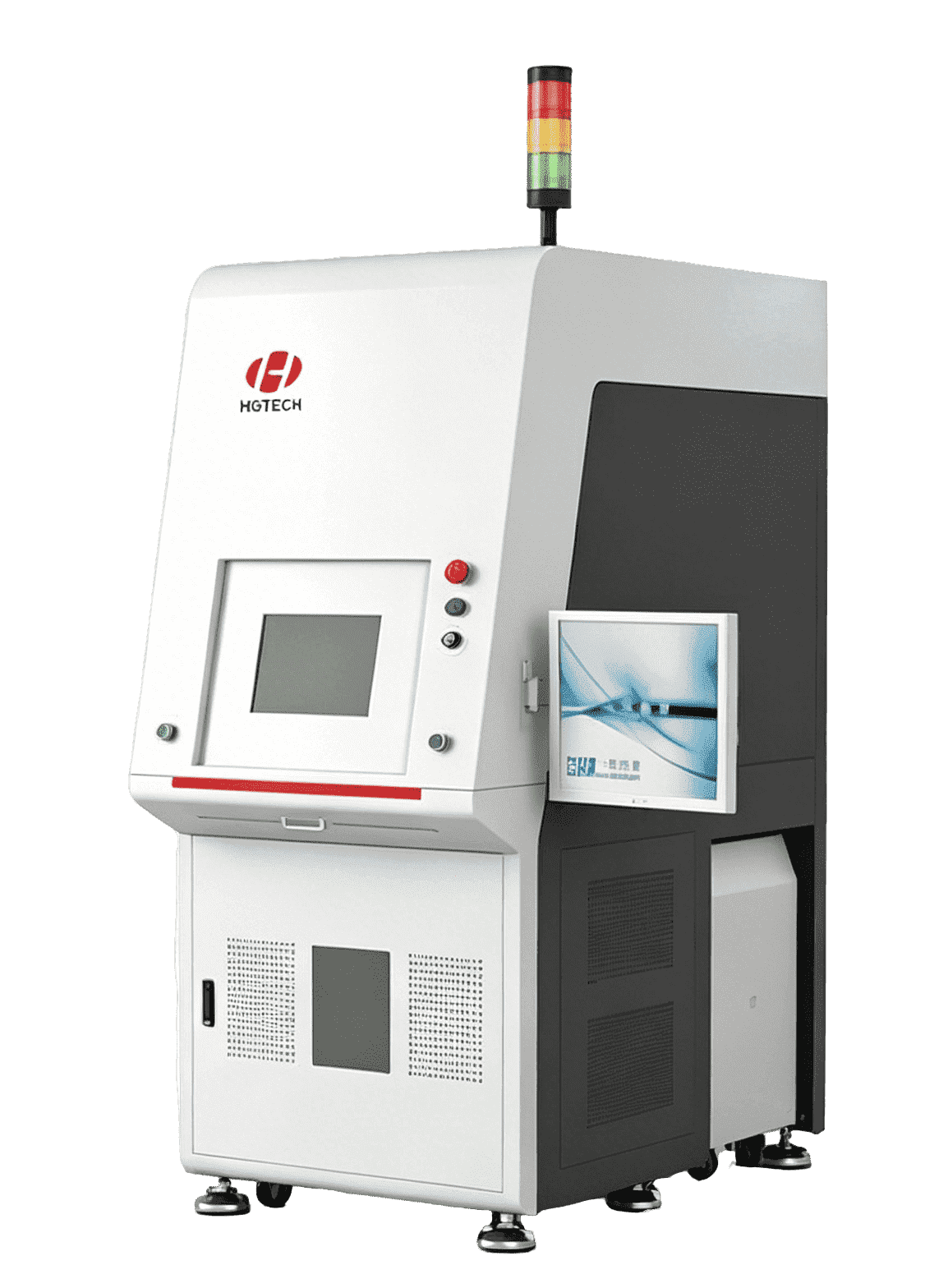
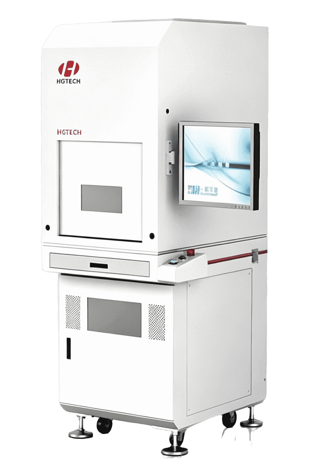
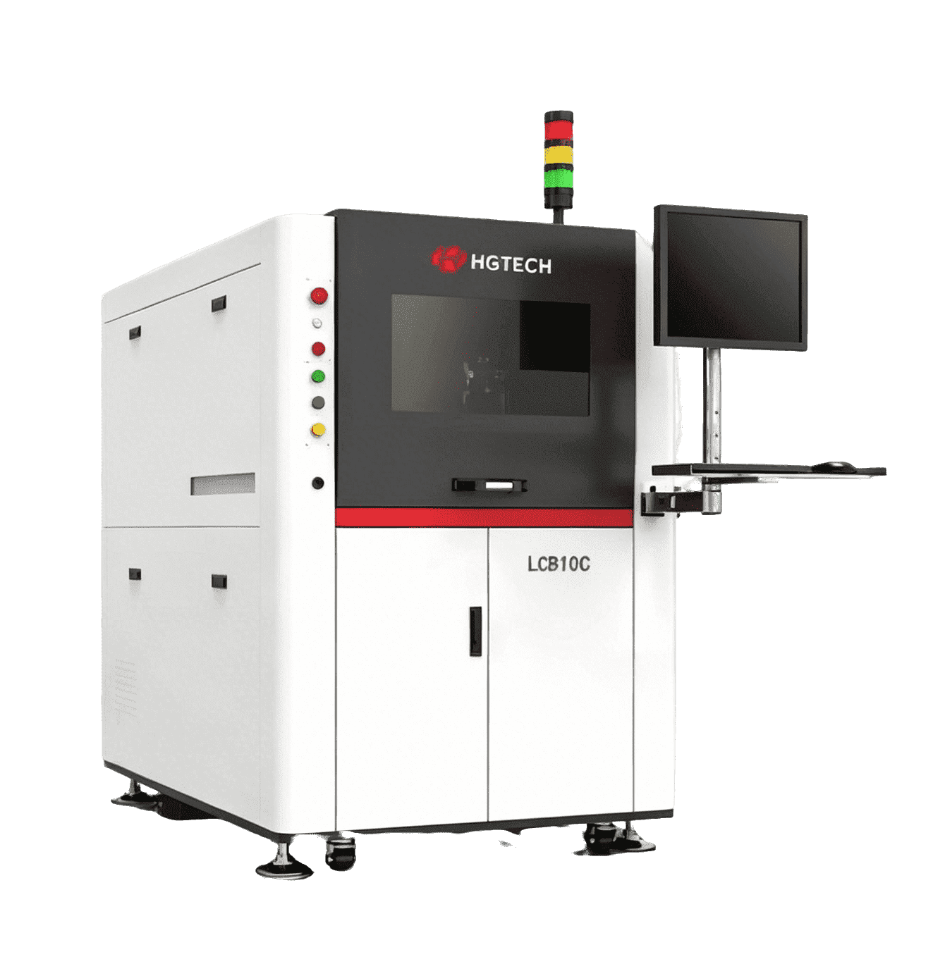
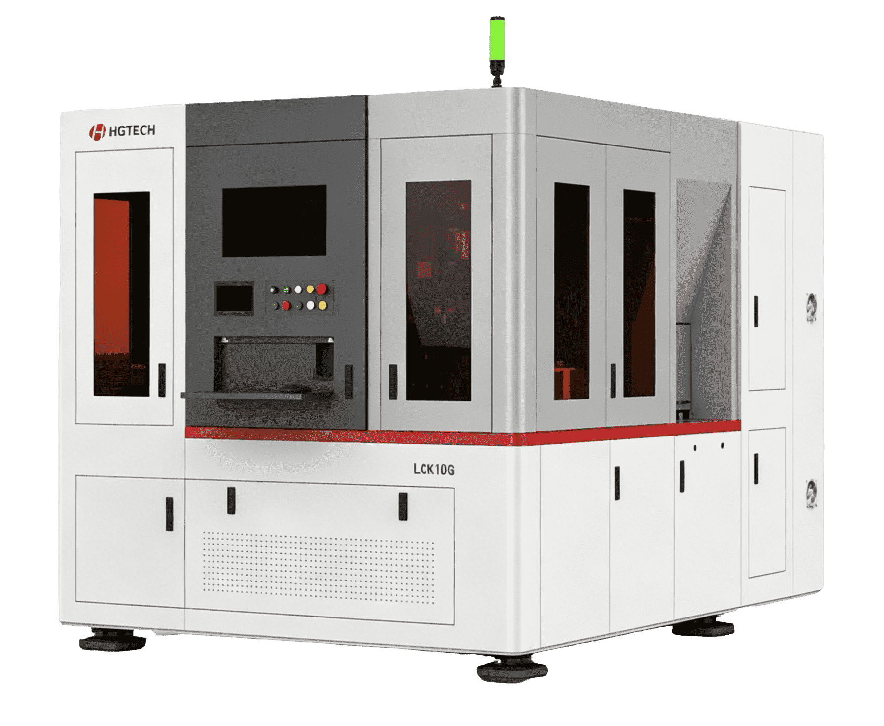
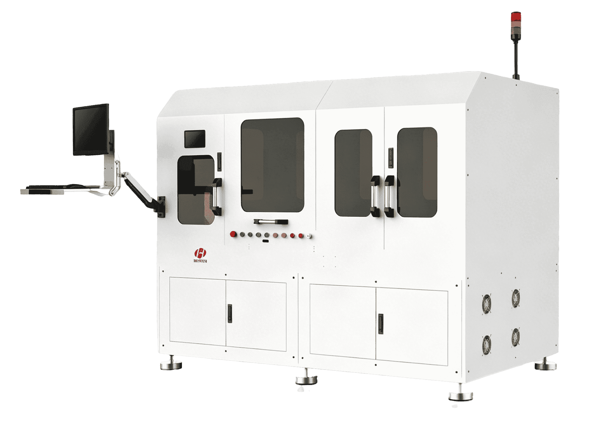
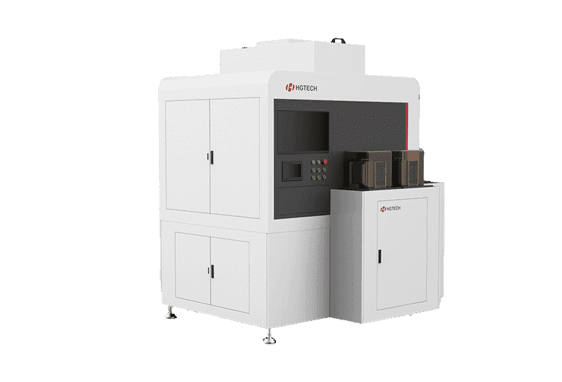
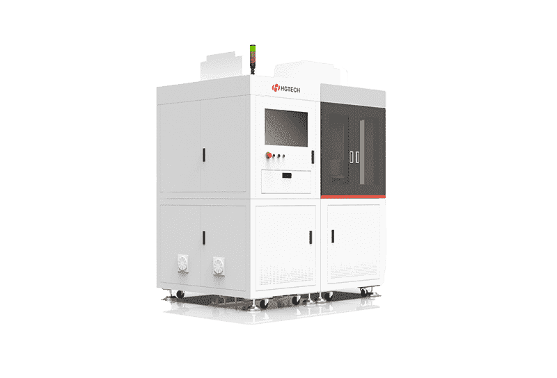
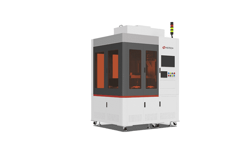
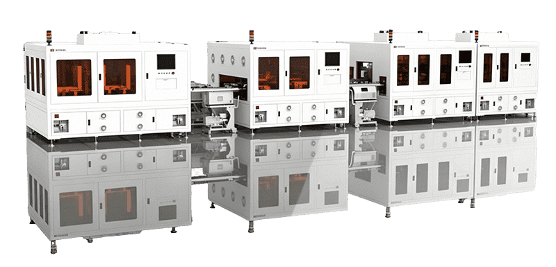
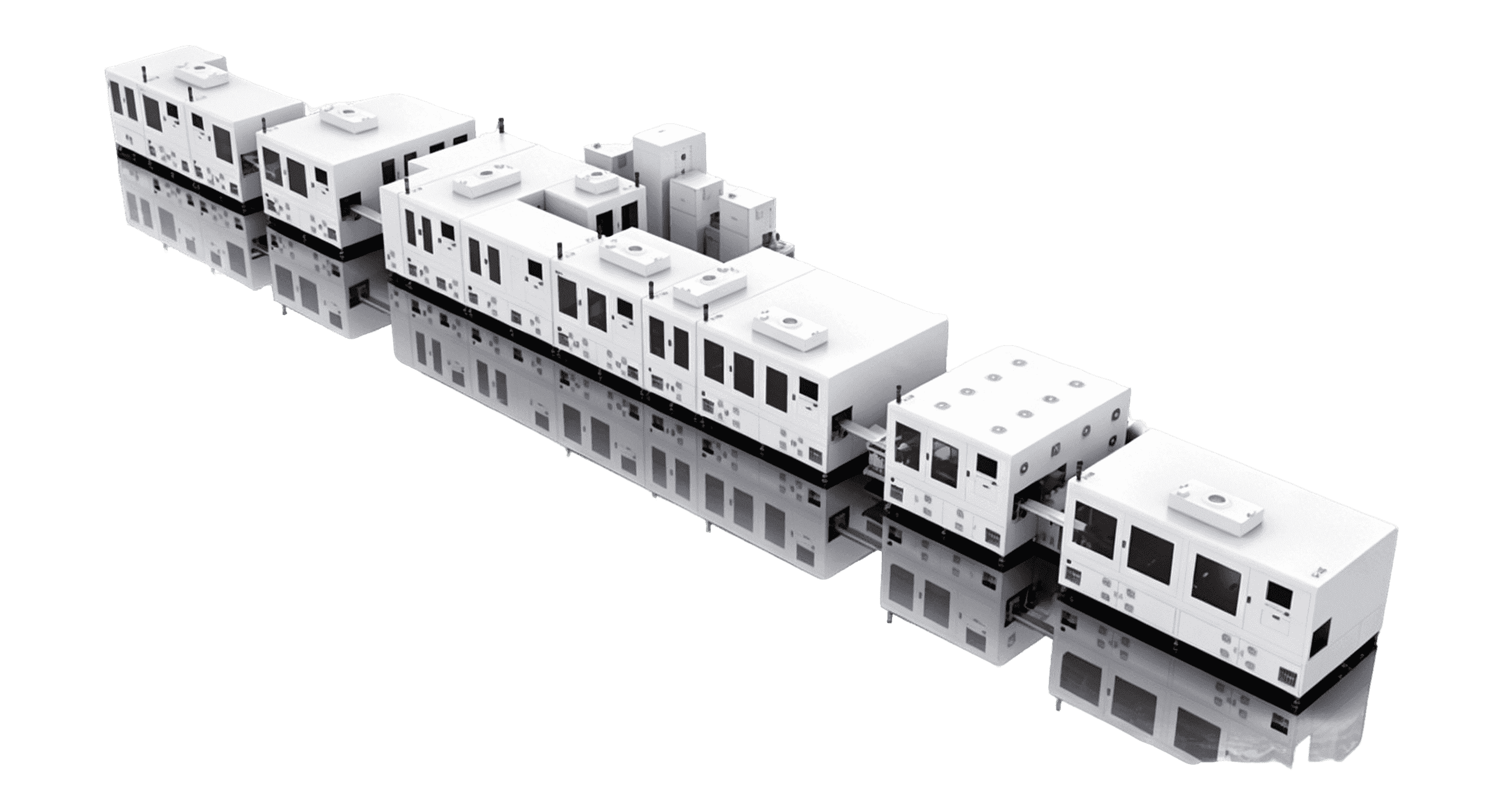
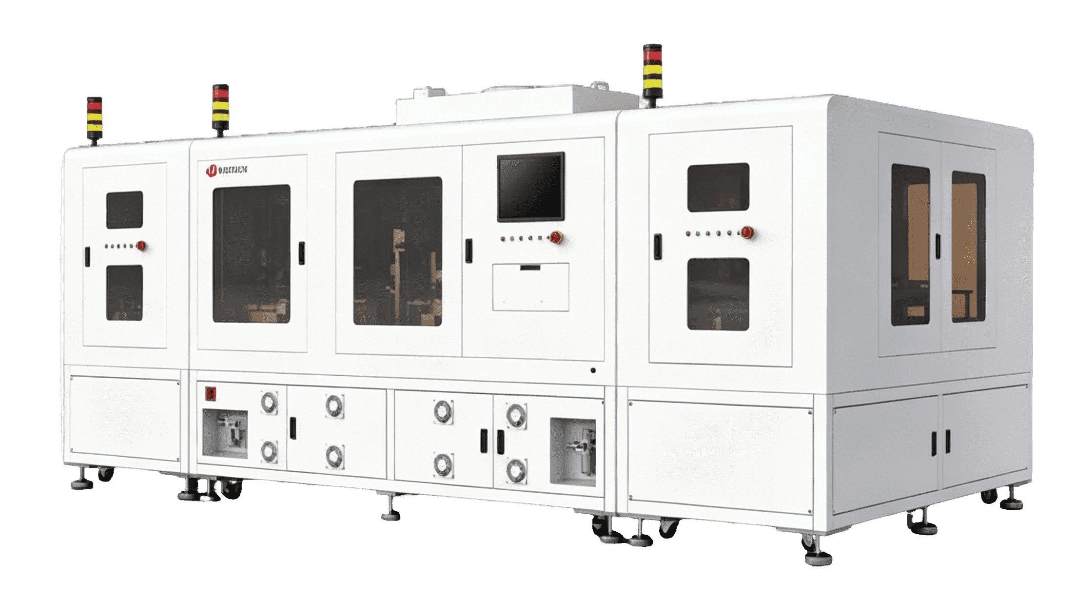
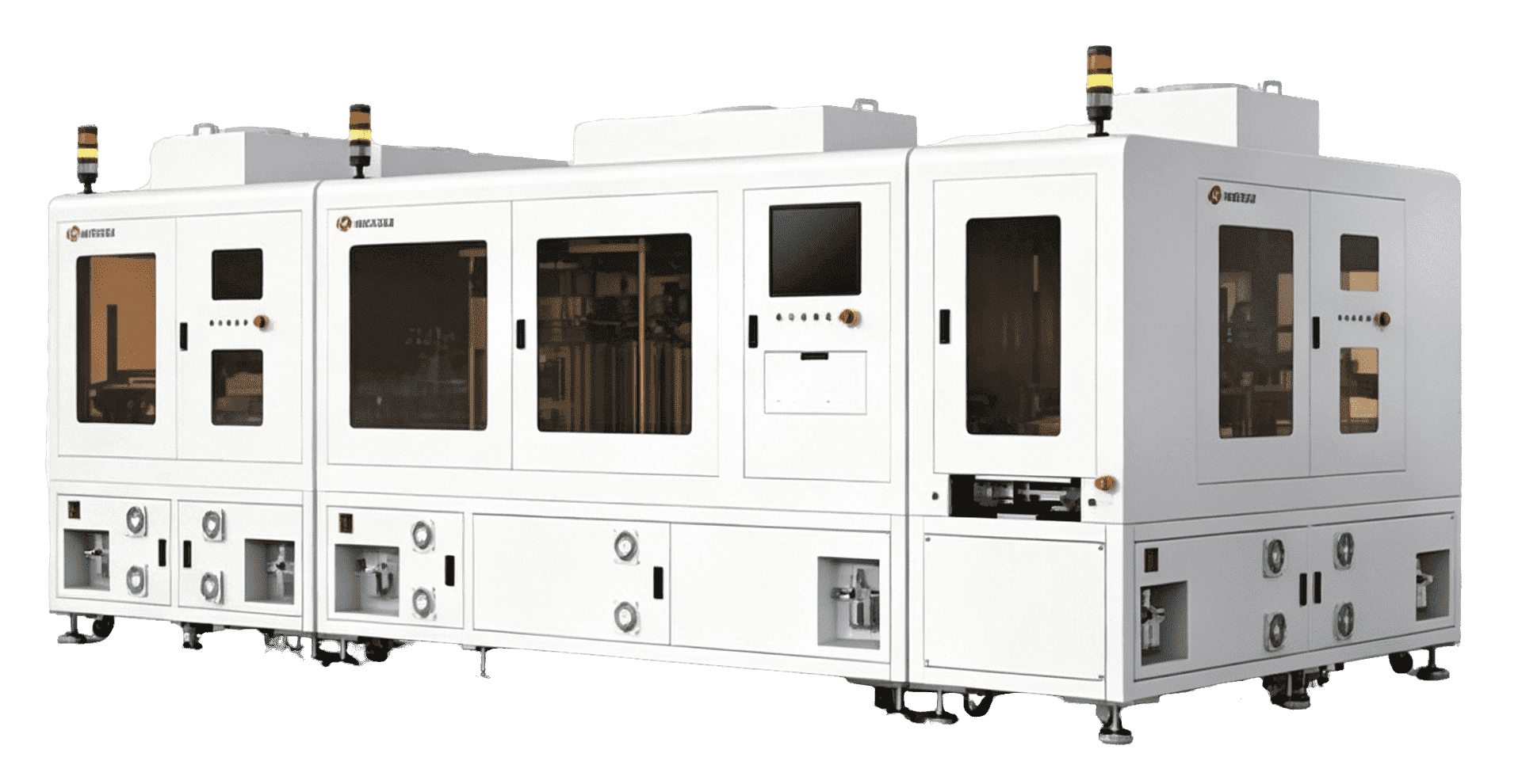
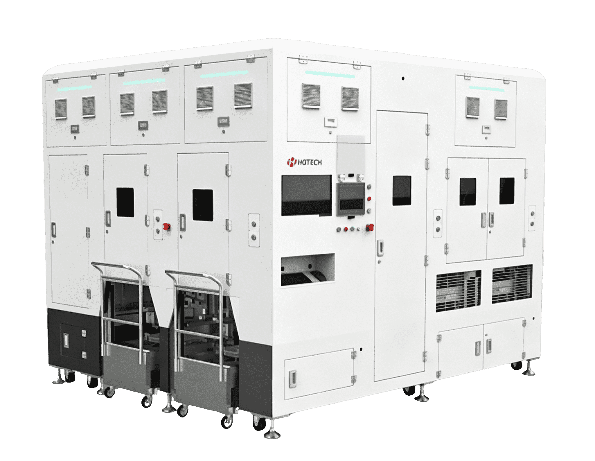
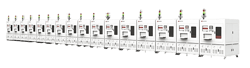
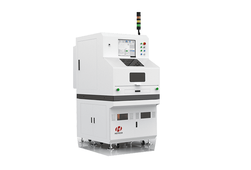
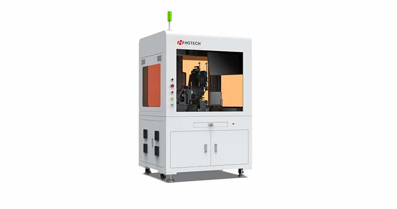
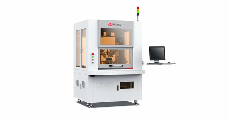
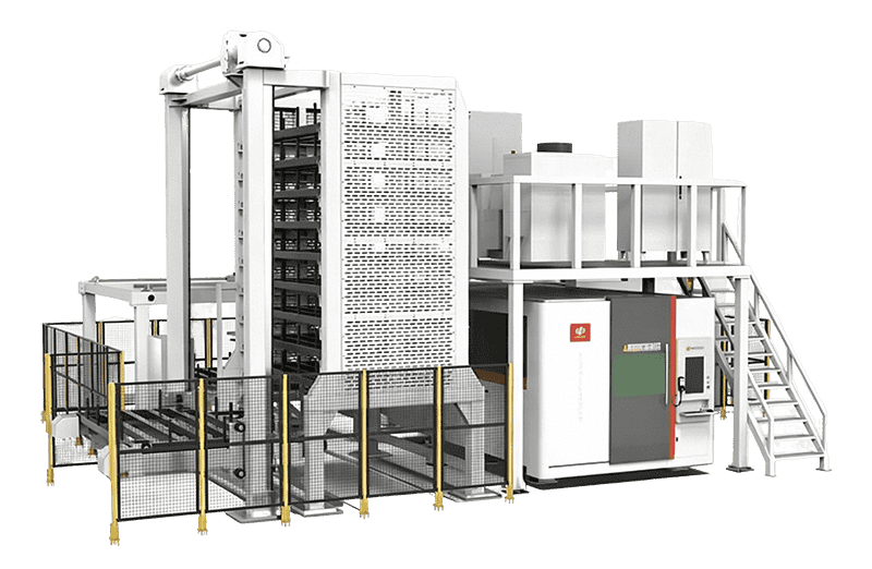
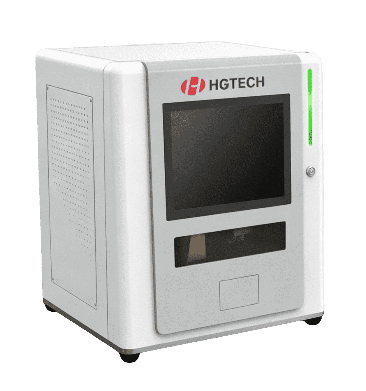
Semiconductor Wafer Thickness Measuring Equipment
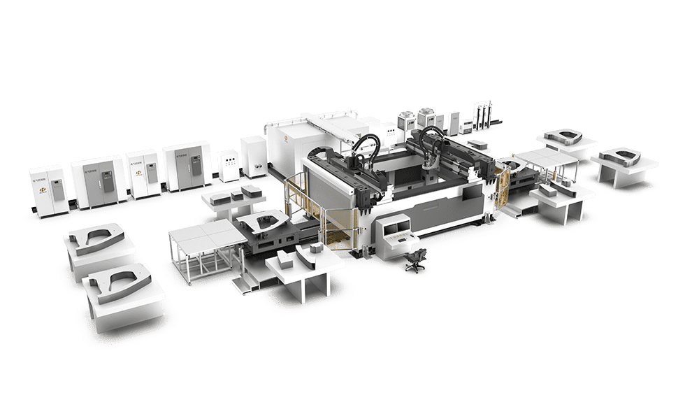
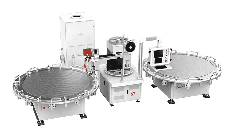
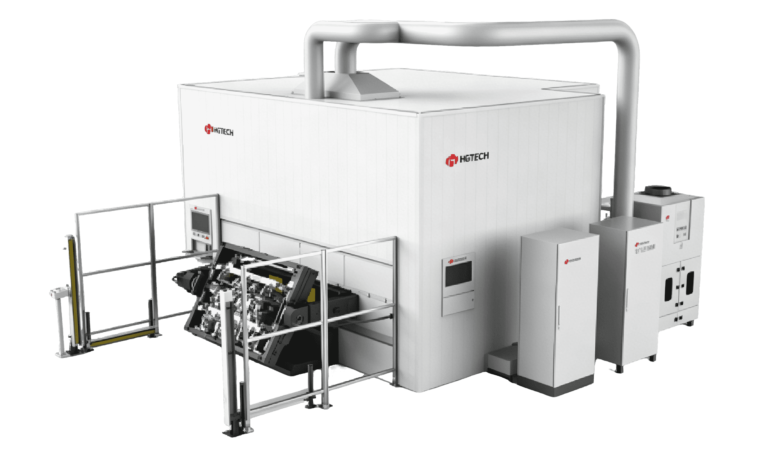
Facing the raw material production enterprises in the upstream of the semiconductor industry chain, the independently developed spectral confocal measurement system is used to detect the size and flatness of semiconductor raw and epitaxial wafers.
Product Consultation

Name *
Company
E-mail *
Phone *
Location *
Main Business
  • Product Description

Product advantages:

  • Wide application range

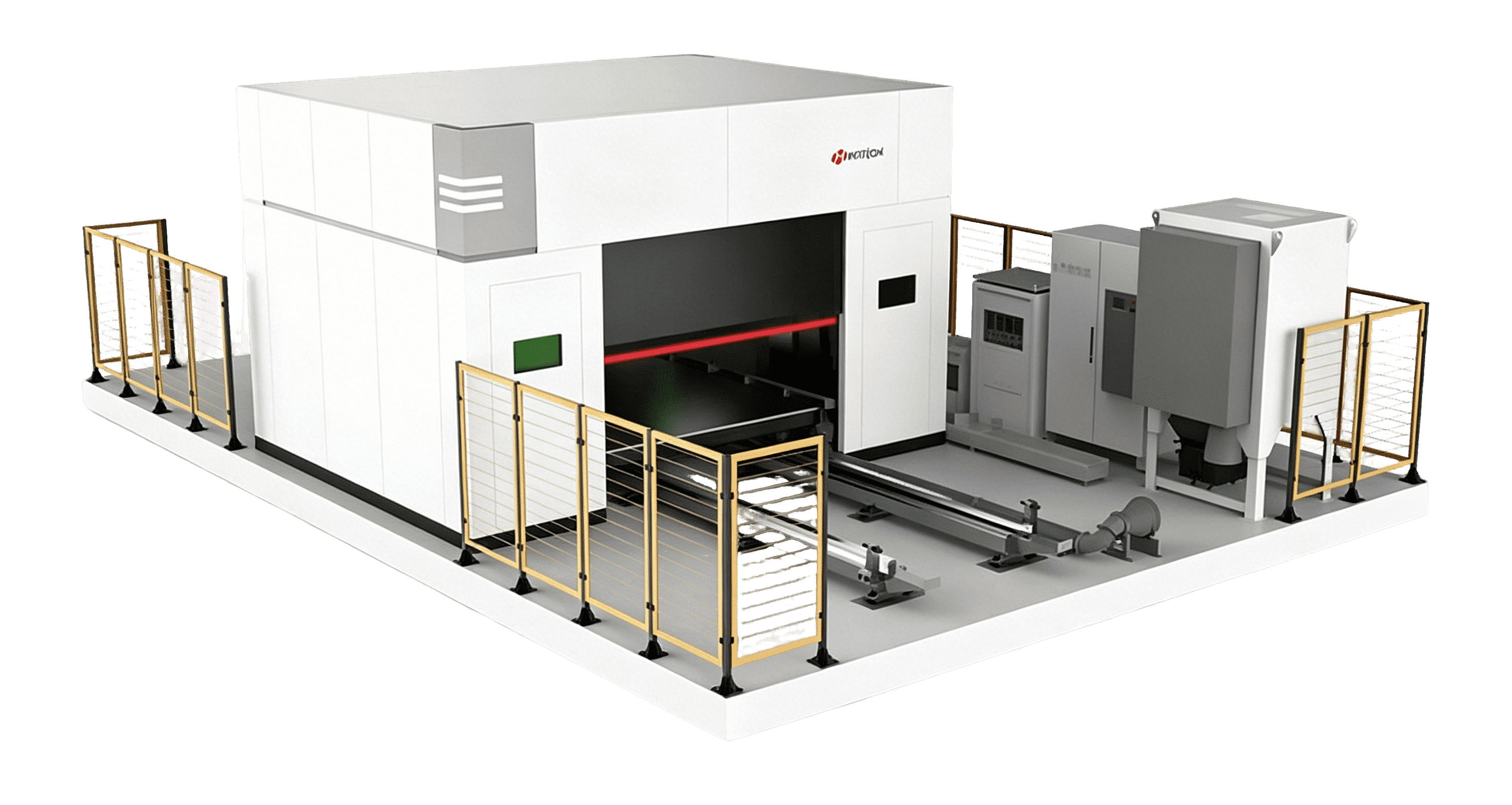
Used for 4-8 inch original wafer, substrate and epitaxial wafer of various materials and polishing conditions
  • High measurement accuracy

Thickness range: 0-1mm measurement accuracy: ± 1 μ M repetition accuracy: 0.2 μ m

  • Short measurement time

Measurement time: 30s / PCS (according to the customer's detection trajectory)
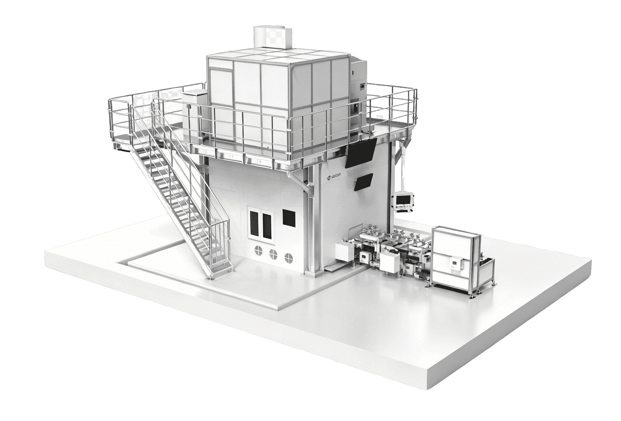
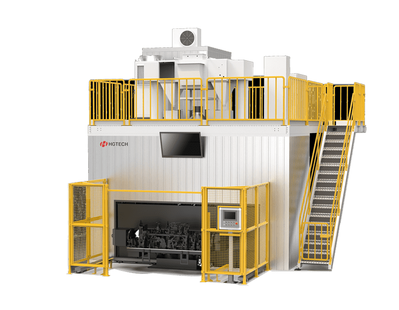
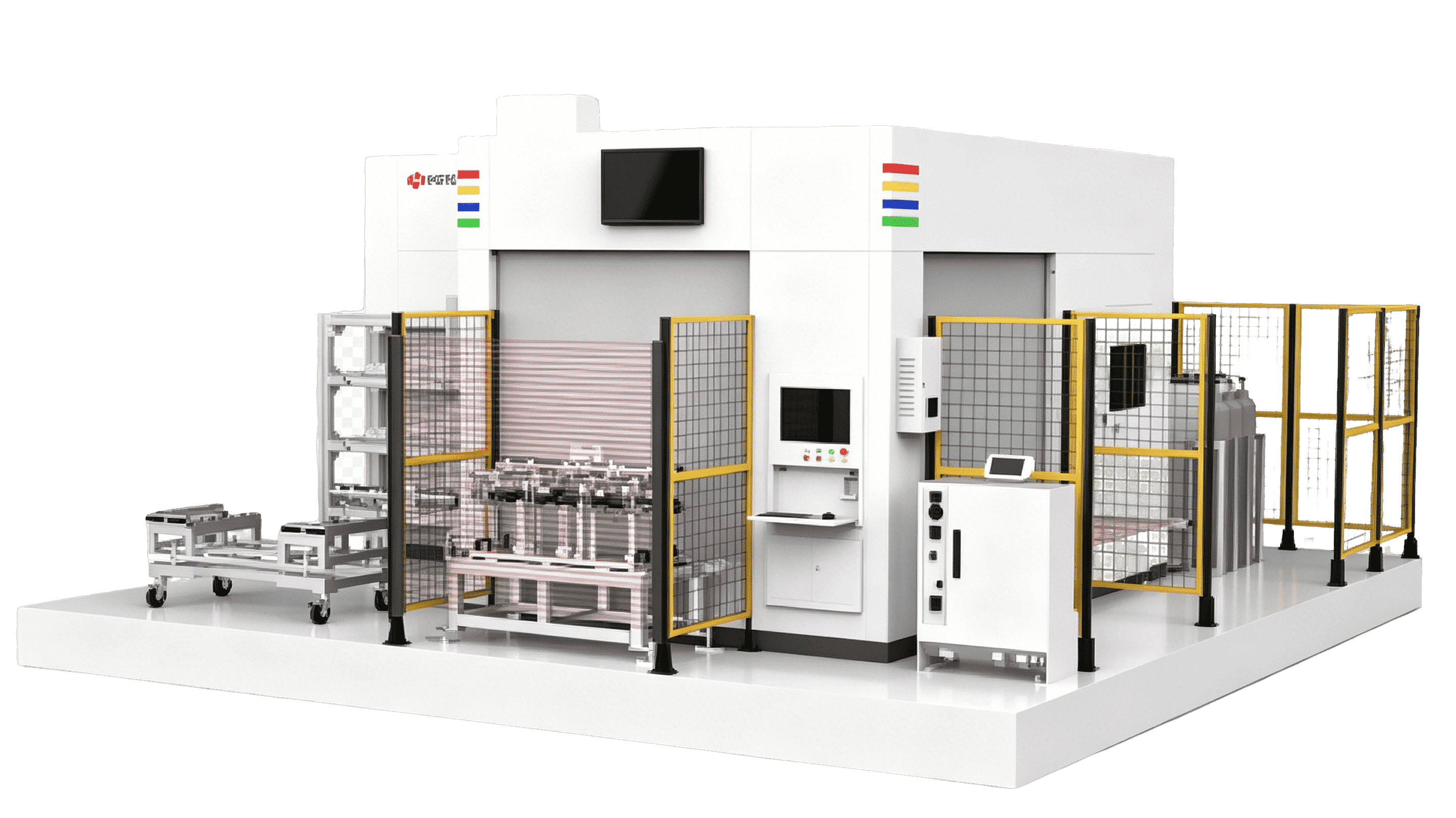
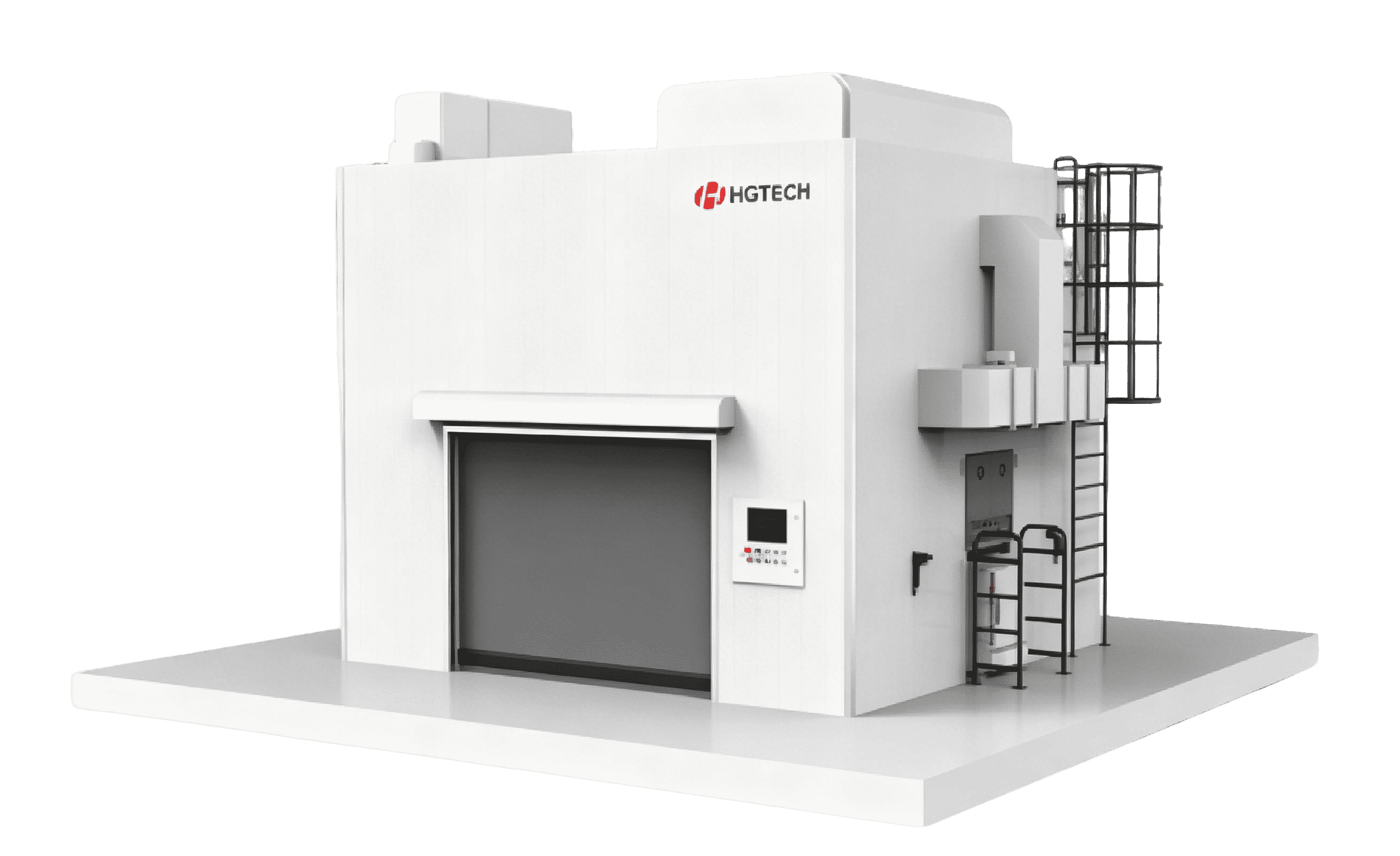
Sample display:

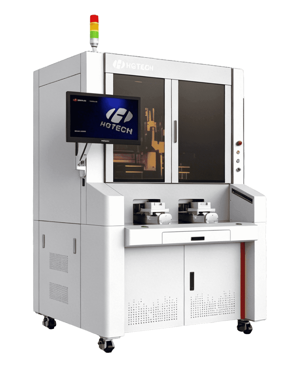
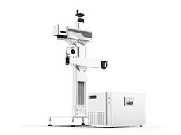
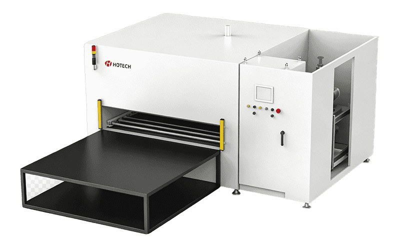
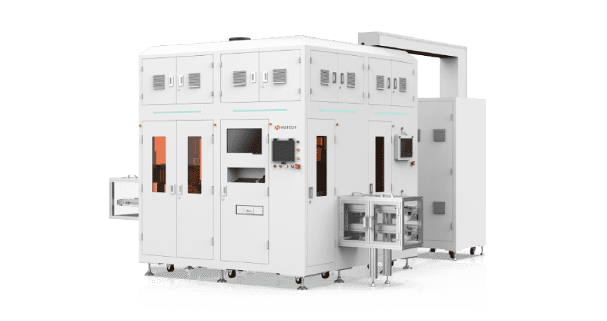
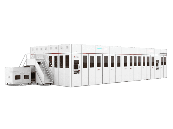
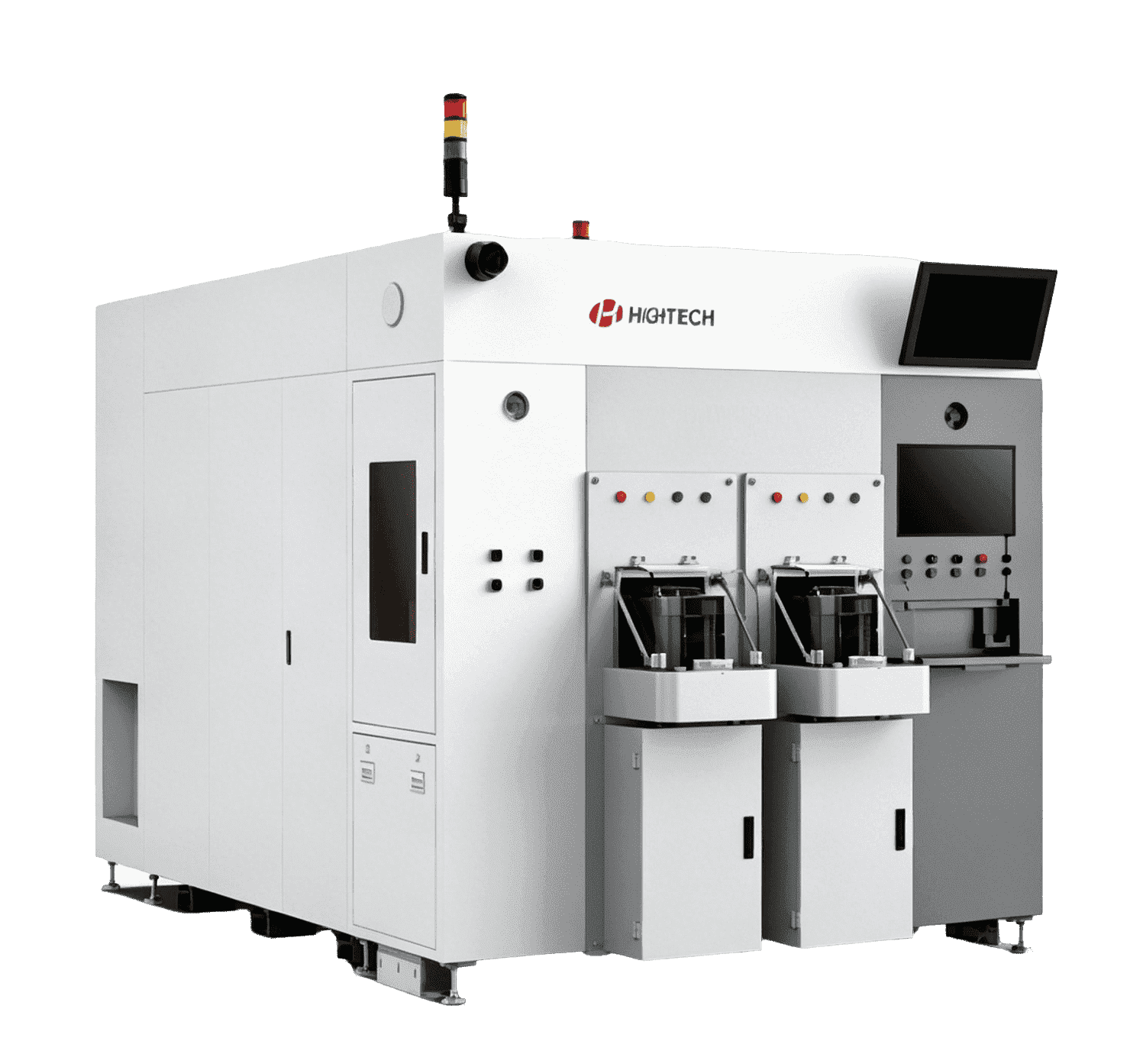
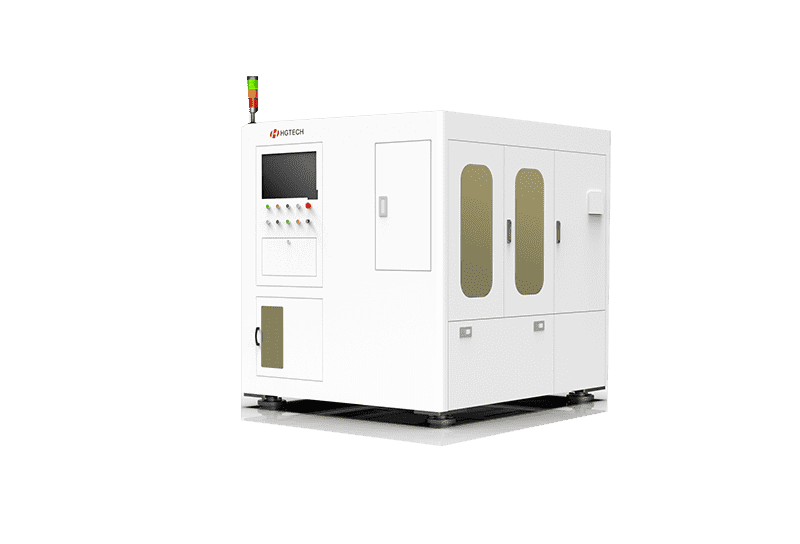
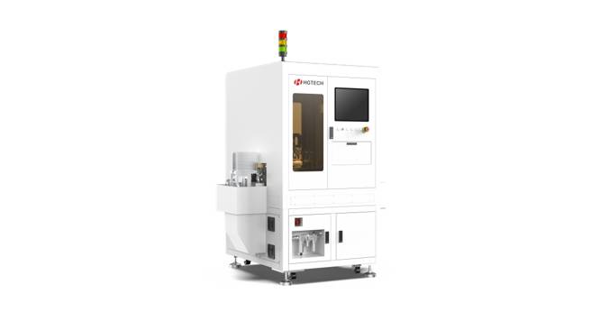
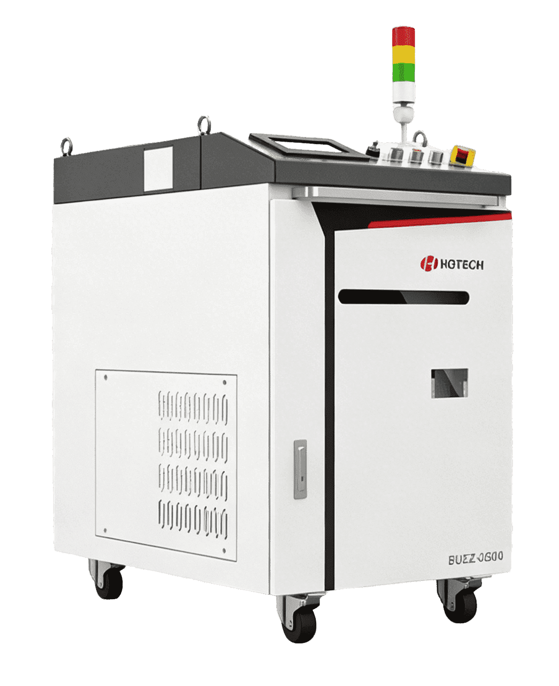
Sample 1

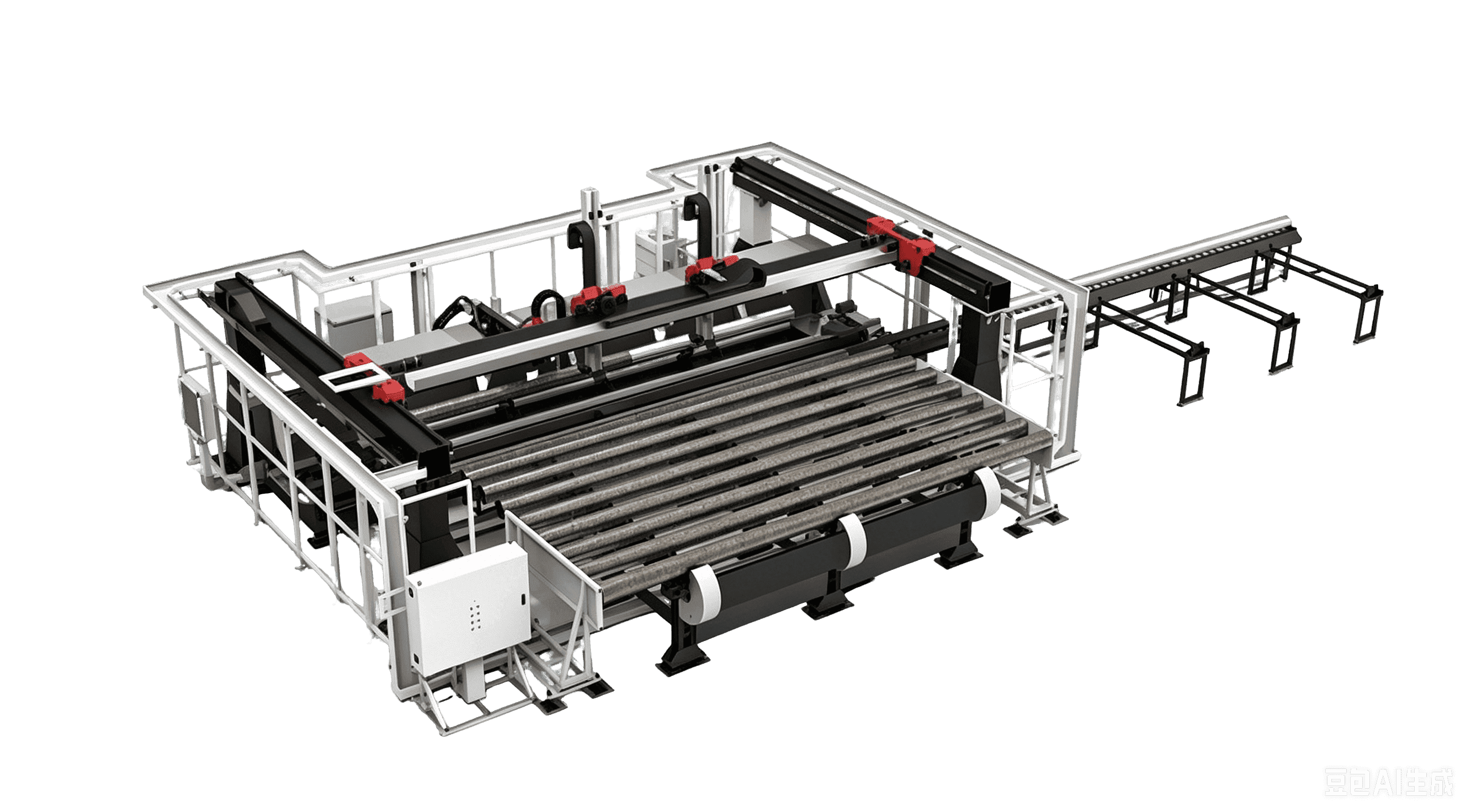
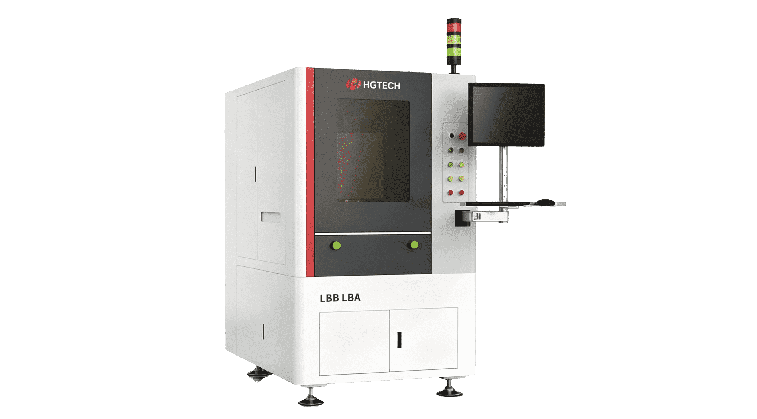
Semiconductor Wafer Thickness Measuring Equipment
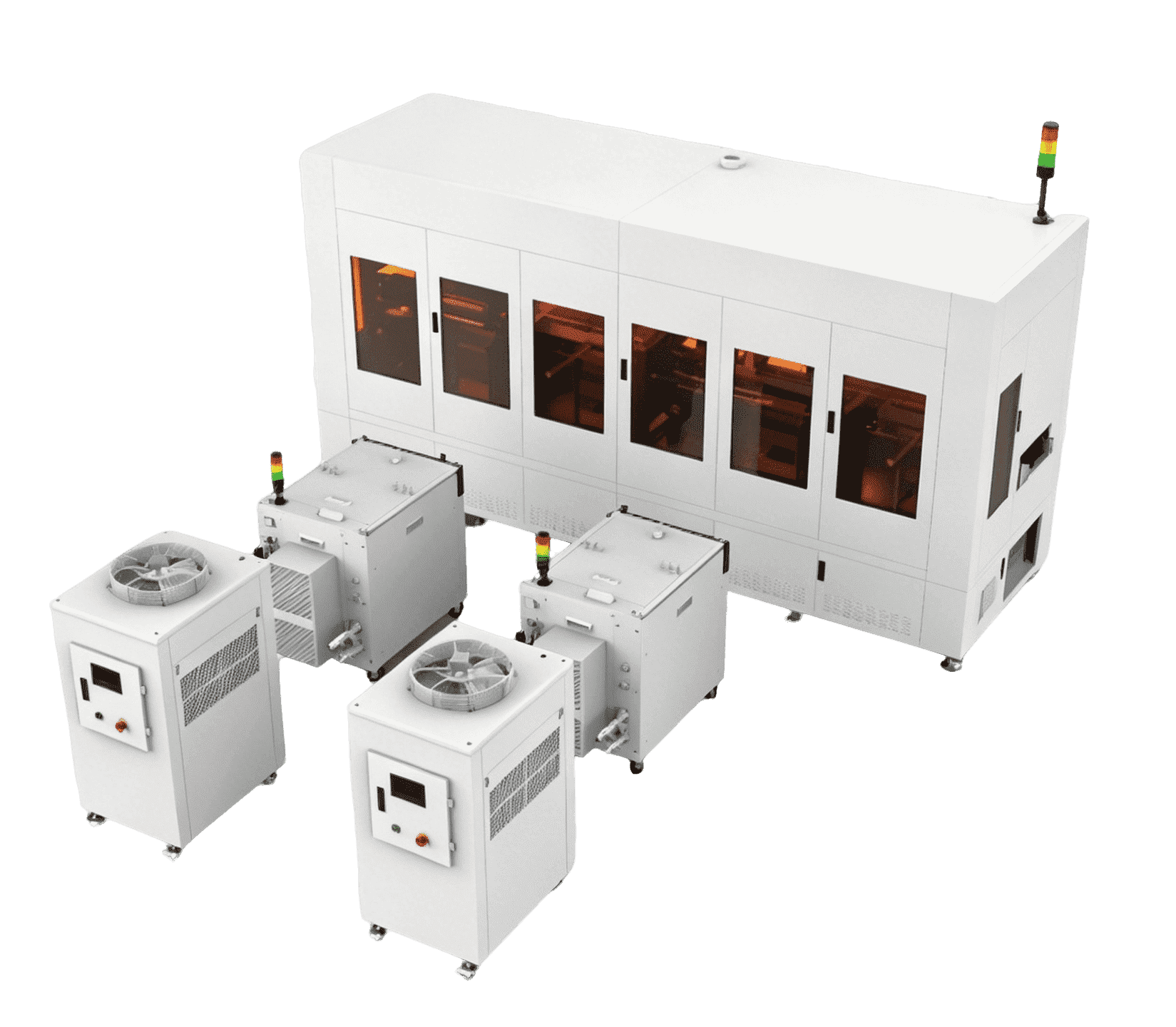
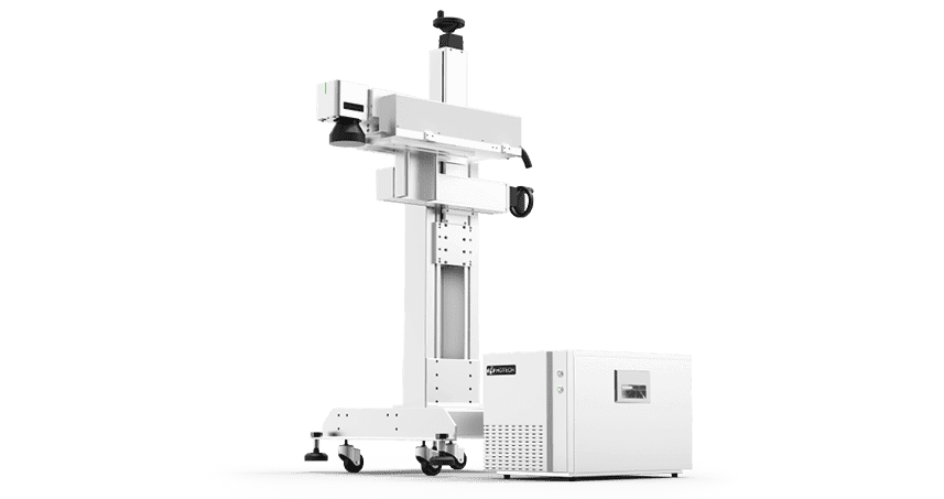
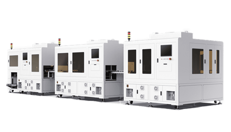
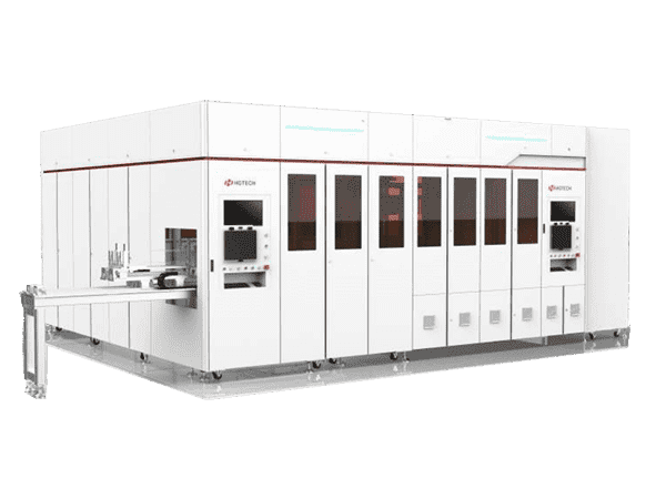
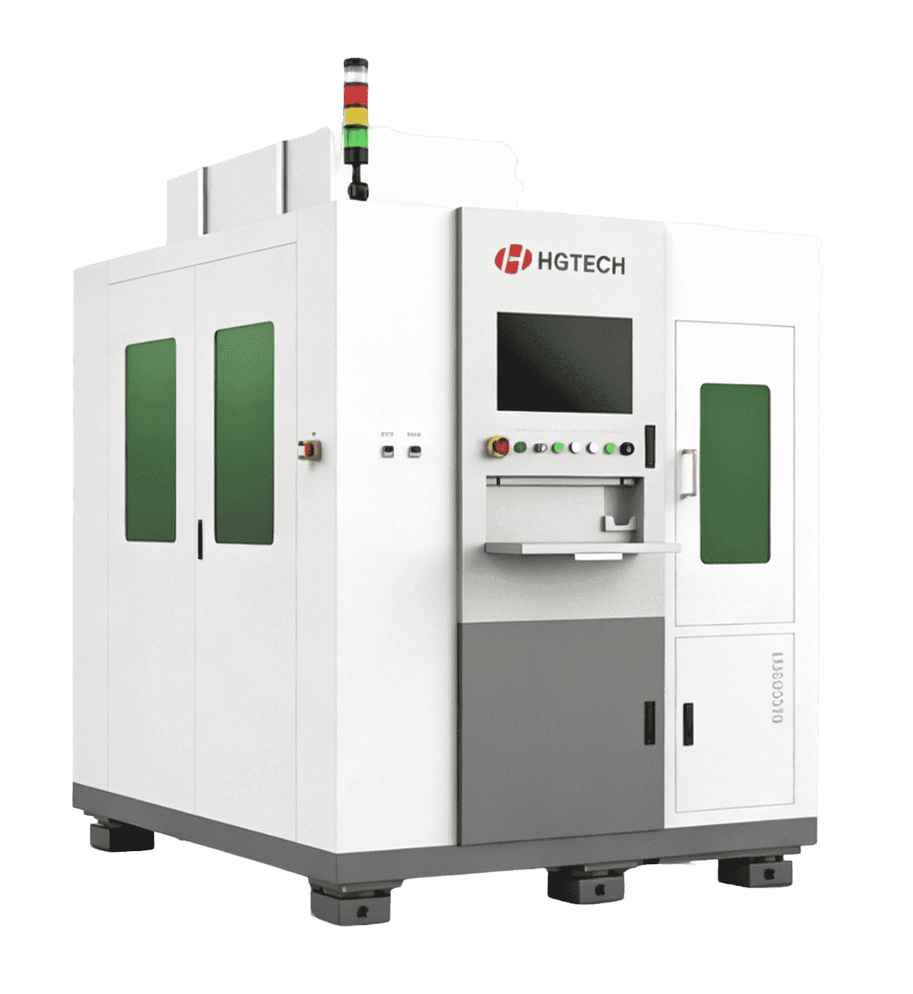
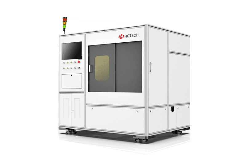
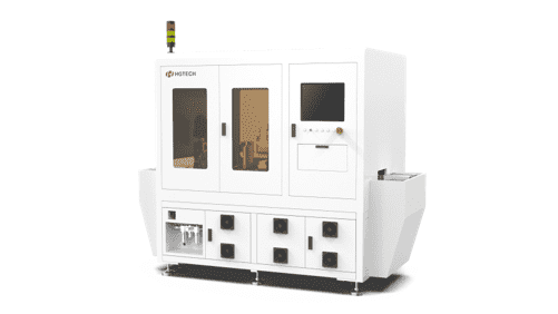
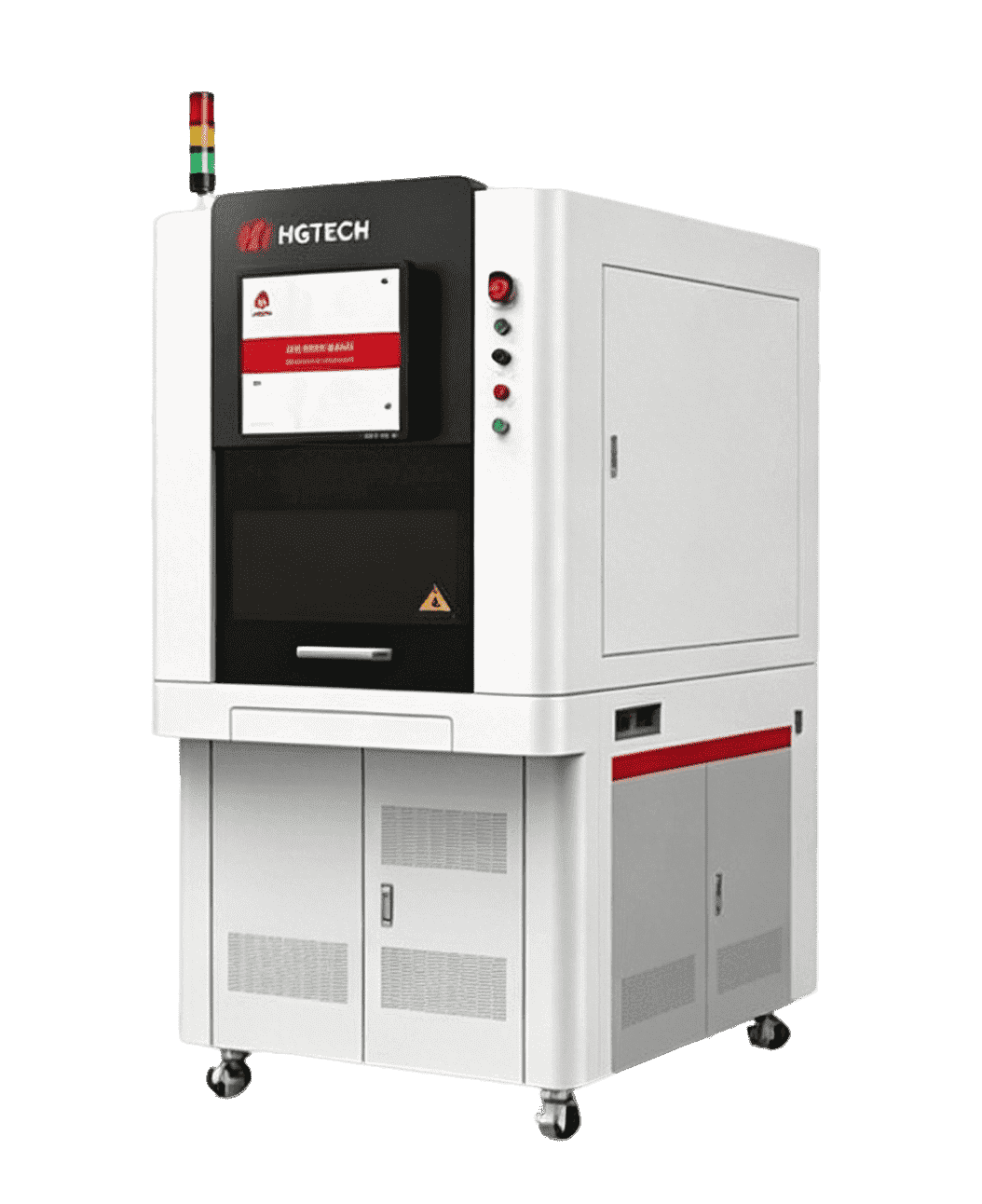
Sample 2

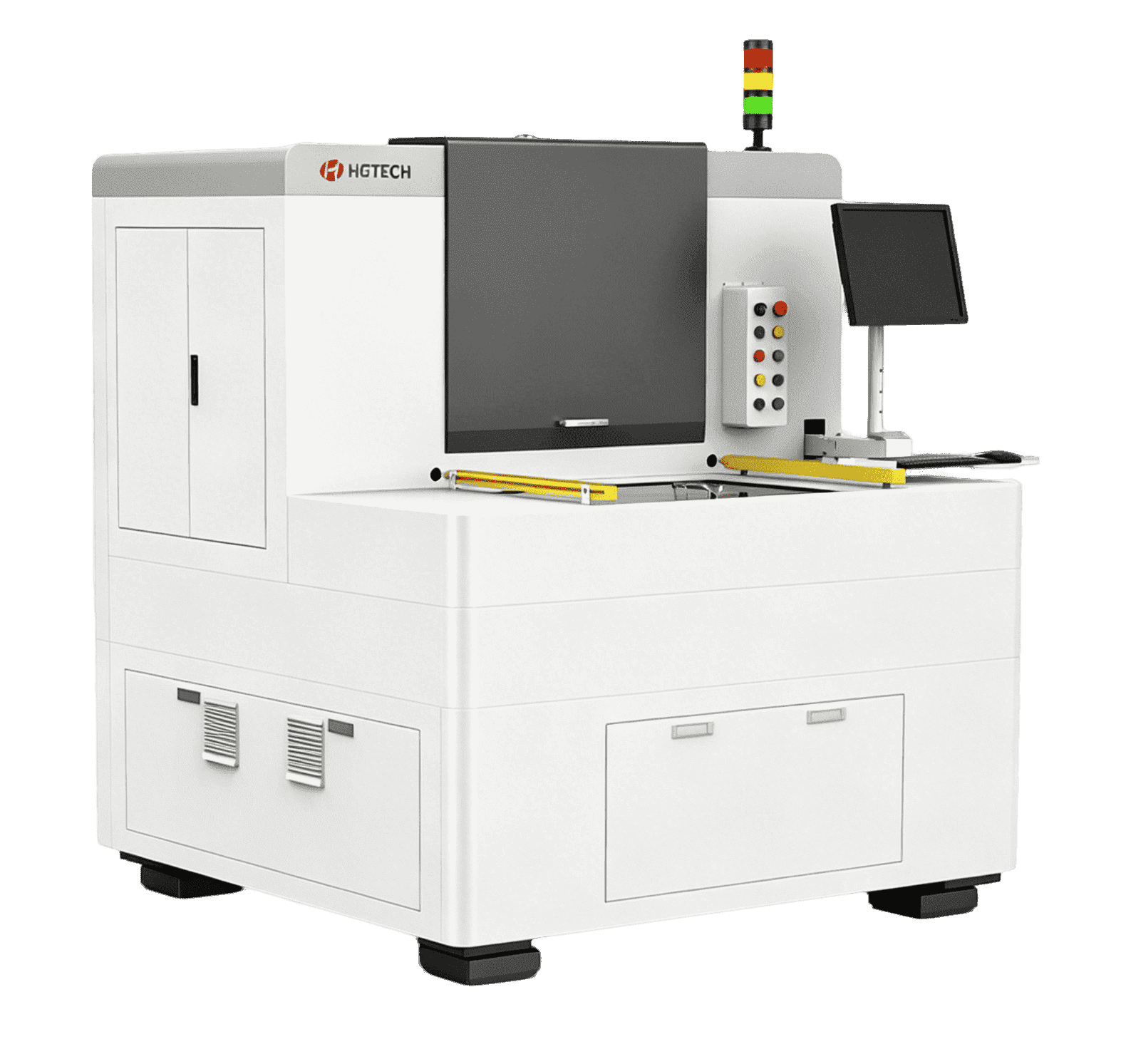
Semiconductor Wafer Thickness Measuring Equipment
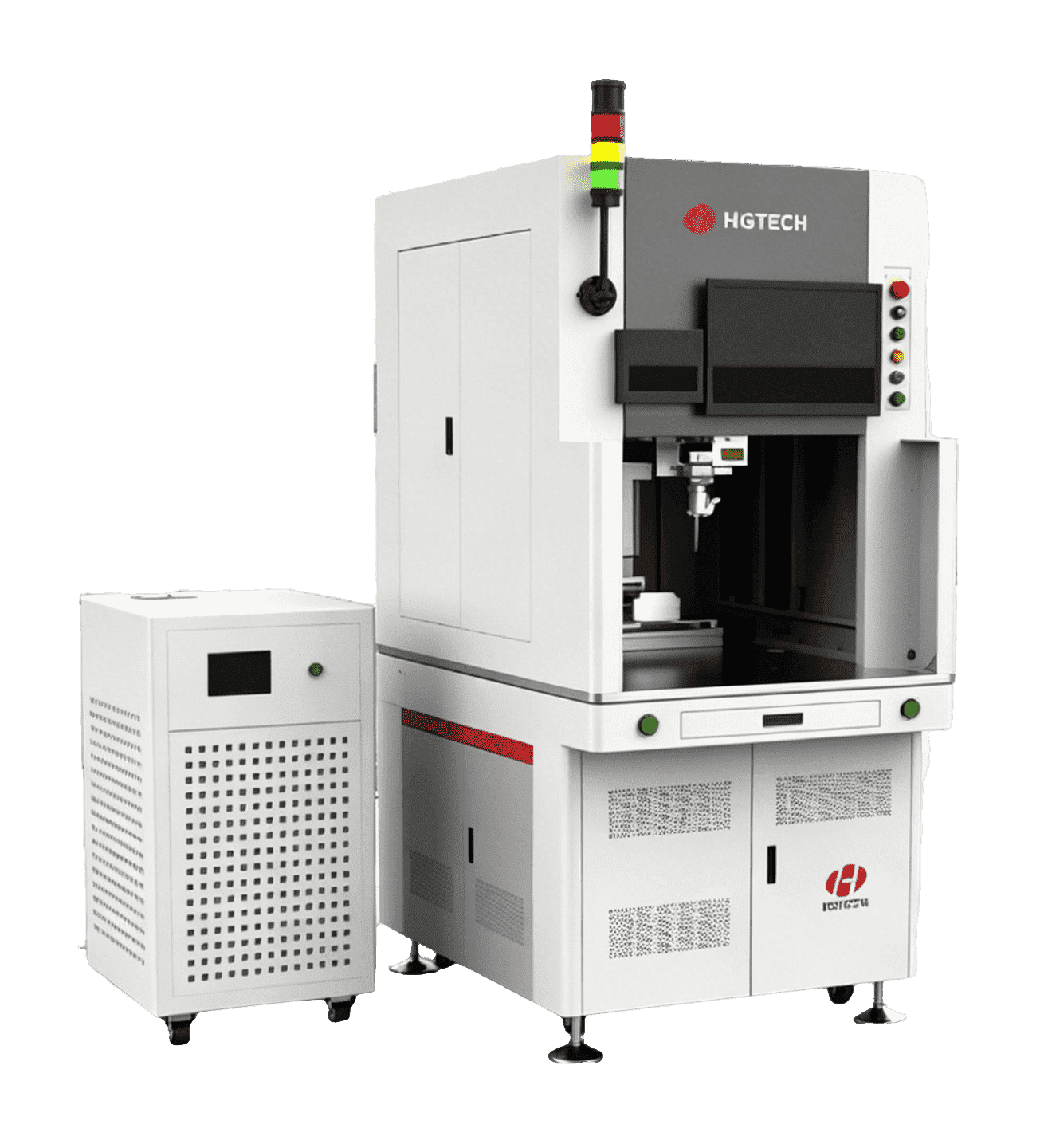
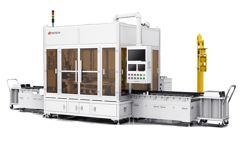
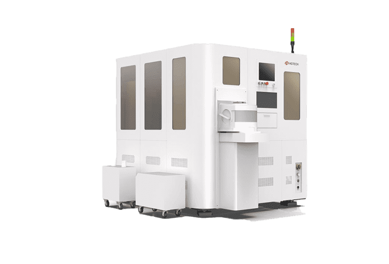
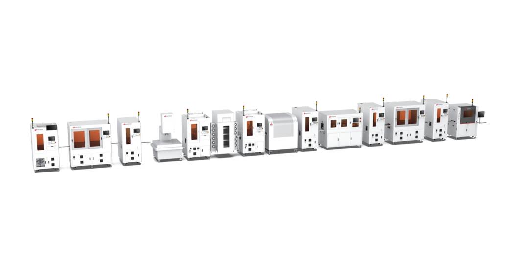
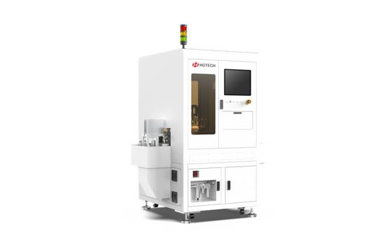
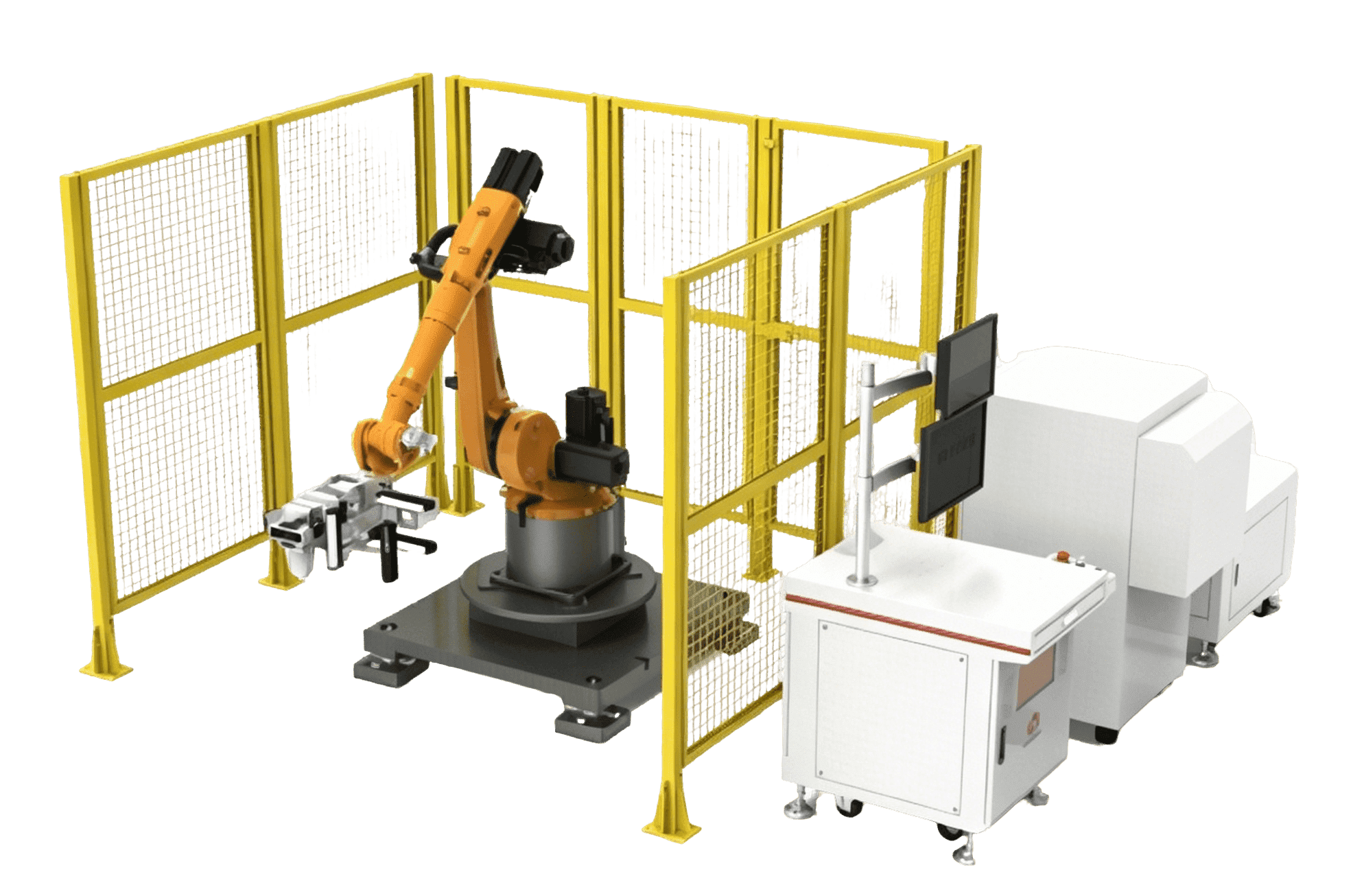
Sample 3

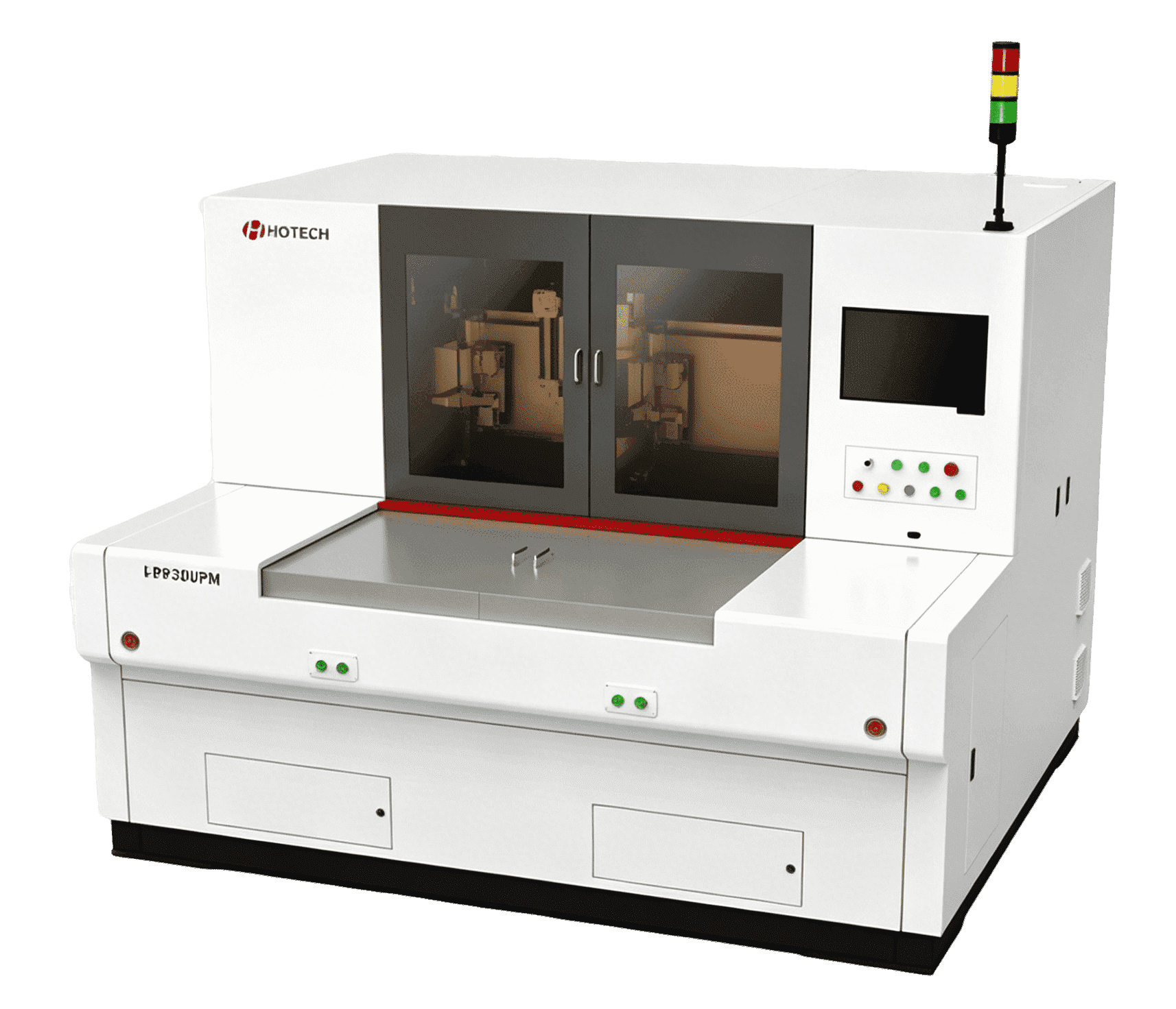
Semiconductor Wafer Thickness Measuring Equipment
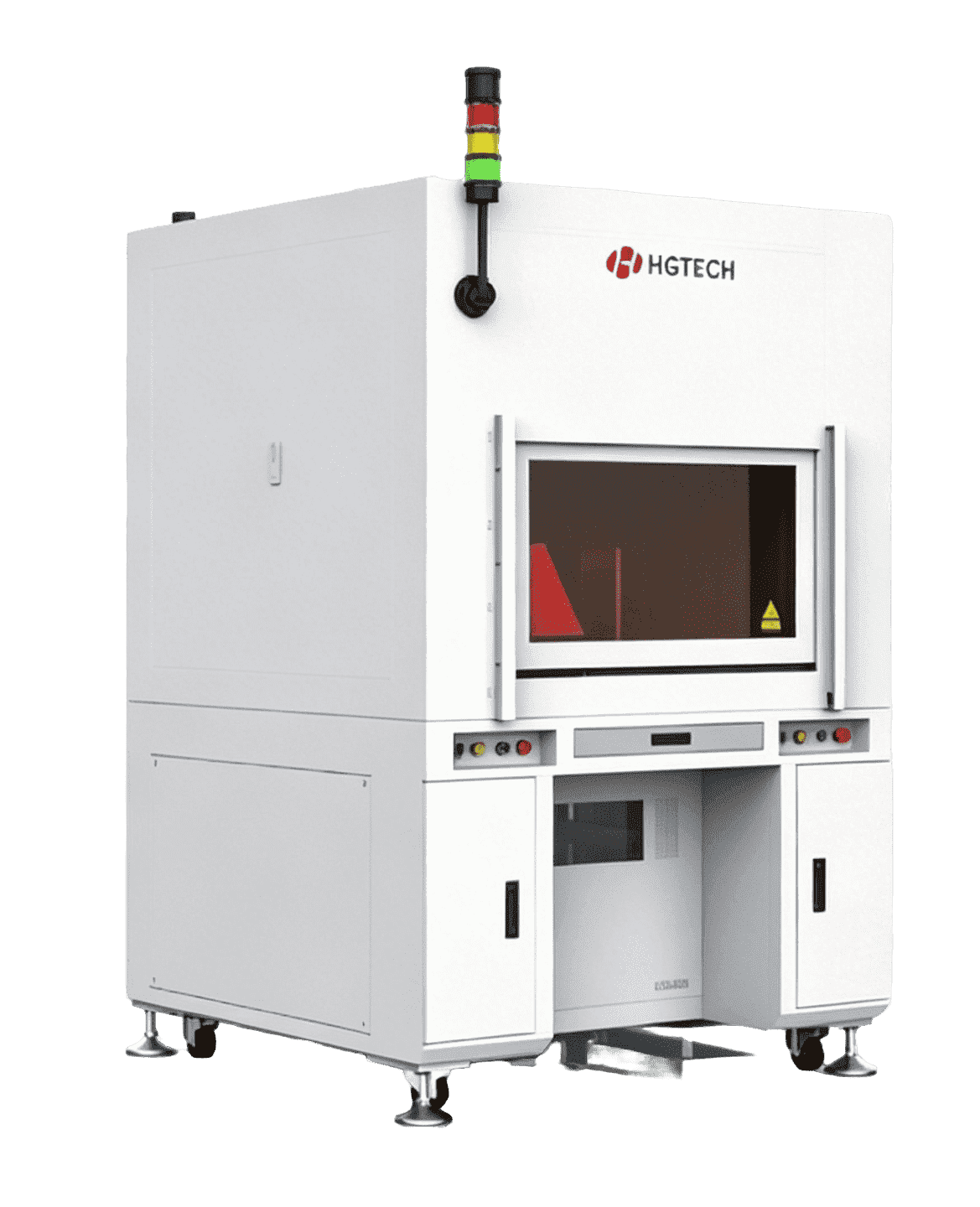
  • Technical Parameters

Item Main parameters
General parameters Wafer size 4", 6"
Number of boxes Double-deck, 14 pcs
Loading and unloading method Robot, mapping scanning
Motion platform X stroke150mm,
Y stroke150mm,
Repetitive accuracy ±0.1 µm
Capacity 4", 240WPH 6", 220WPH
Detection performance Detection function Wafer (coated wafer) thickness, TTV, warpage
Thickness test accuracy ±0.5 µm. Repeatability: 0.1 µm (25 pieces continuously tested, 5 points for each piece)
Thickness range ± 1 mm
TTV test accuracy ± 0.5 um, repeatability: 0.2 µm
Warpage test accuracy ± 2 µm. Test range: ± 600 µm. Repeatability: 1 µm
Environment requirement Power supply specification AC220V,50Hz
Air source requirements 0.5-0.7mpa compressed air, without obvious water vapor and grease
Using environment Temperature: 15-40 ℃. Humidity requirement: 30% - 70%, no frost
Overall size 1800mm*1300mm*2250mm

Message Form

Name *
Company
Country *
Model
E-mail *
Phone *
Message