
HGTECH 武汉华工激光工程责任有限公司 privacy policy
Copyright HGLaser Engineering Co,.Ltd. All Rights Reserver.
As AI transitions from technology validation to mass production, the yield, efficiency, and scalability of hardware manufacturing have become critical factors shaping the future of the AI industry.
HGLaser launches the “AI Intelligent Manufacturing Deep Dive” series, providing an in-depth exploration of intelligent manufacturing solutions for the AI industry chain — from equipment technologies and process innovation to production line implementation.
Through this series, HGLaser demonstrates how its advanced laser processing technologies and intelligent manufacturing capabilities help customers overcome mass production challenges and provide advanced manufacturing capabilities for the global AI ecosystem.
With the continuous evolution of large-scale AI models and multimodal AI technologies, the global AI industry chain is undergoing a major transition from technology validation to mass production.
Leading AI semiconductor companies are accelerating next-generation computing capabilities through heterogeneous integration architectures based on chiplet + HBM3e. However, true industrial-scale AI deployment depends not only on advanced computing chips, but also on building a stable, efficient, and scalable AI hardware manufacturing ecosystem.
From AI computing infrastructure and high-speed data transmission to edge applications, the manufacturing capability of every critical hardware component directly impacts the speed and scale of AI’s transition from cloud computing to real-world applications.
Facing these industrial challenges, HGLaser leverages years of expertise in laser processing and intelligent manufacturing to develop comprehensive intelligent manufacturing solutions covering key segments of the AI industry chain.
This article focuses on three critical application fields — advanced packaging substrates, high-speed connectors, and optical waveguides — highlighting HGLaser’s technological breakthroughs in AI computing infrastructure, high-speed data transmission, and next-generation optical interaction components.
Advanced packaging substrates are critical materials for semiconductor packaging and represent one of the sectors with the highest technological complexity and strongest growth potential in the global semiconductor supply chain.
Driven by the rapid development of AI computing chips toward higher computing performance, bandwidth, and integration density, advanced ABF and BT substrates have become essential components for AI servers and accelerator cards.
Modern substrate manufacturing has reached 10 μm-level line/space, with layer counts increasing to 12–20 layers. Advanced processes such as microvias and high-density interconnect (HDI) structures have introduced increasingly demanding requirements for processing precision, process stability, and end-to-end traceability.
Traditional manufacturing methods are no longer sufficient to support high-volume production requirements.
• Laser marking and traceability code conversion
After inner-layer information is embedded through lamination processes, original identification data may be lost, creating challenges for end-to-end traceability. More than 30% of production batches may fail to meet the traceability requirements of high-end customers.
• Defect identification and marking
Manual defect marking suffers from inconsistent quality, with qualification rates below 70%, while lacking comprehensive digital records.
• Intelligent sorting and packaging
Manual inspection and sorting result in high false detection and missed detection rates of 5%–8%, while dust contamination contributes to unnecessary yield loss.
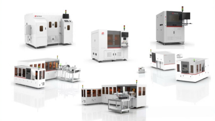
Designed for AI chip-related organic substrates (ABF/BT substrates), HGLaser’s intelligent manufacturing solution targets critical back-end processes in advanced packaging substrate production.
The solution integrates:
• Inner-layer substrate laser marking and traceability code conversion
• Precision defect identification and marking
• Intelligent sorting and automated packaging
By combining laser processing, intelligent inspection, and automation technologies, HGLaser creates a fully digitalized manufacturing workflow that supports advanced packaging applications such as AI chiplet integration and HBM stacking.
Core Advantages:
The solution integrates innovative X-ray-based buried code reading and laser precision code conversion technology, effectively addressing traceability challenges affecting more than 30% of production batches.
Through comprehensive mapping-based data management, every manufacturing stage becomes fully traceable.
By combining intelligent vision inspection with laser marking technology, the solution significantly reduces inspection losses caused by manual errors, helping improve substrate production yield from below 90% to over 99%.
It provides an efficient solution to the key challenges of quality control, traceability, and high-volume production for advanced ABF/BT substrates.
High-speed connectors are critical components for transmitting high-frequency and high-speed signals in AI servers and advanced communication systems.
With the rapid growth of 5G communications and AI computing, data transmission speeds have reached the Gbps level, making signal integrity, reliability, and interference resistance essential performance requirements.
Three Major Manufacturing Challenges:
• Wire stripping
Ultra-fine wires are highly vulnerable to mechanical damage during processing.
• Precision laser welding
Highly reflective thin-wall materials such as copper alloys are prone to welding defects including spatter and incomplete fusion.
• Weld quality inspection
Micro weld joints measuring 0.1–0.6 mm may contain hidden defects that are difficult to detect through manual inspection.
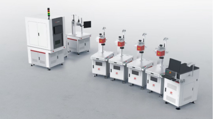
Designed for precision manufacturing of:
• High-speed backplanes
• Midplanes
• I/O connectors
• Cable assemblies used in 5G communications systems and AI servers
HGLaser’s solution covers key manufacturing processes including:
• Wire stripping
• Terminal laser welding
• Post-weld quality inspection
Core Advantages:
The solution overcomes micron-level welding challenges for highly reflective materials such as copper alloys.
Through the Laser Welding Monitoring (LWM) real-time quality monitoring system, it enables “welding while monitoring,” ensuring every micron-level weld joint meets the stringent signal integrity requirements of the AI era.
Optical waveguides utilize total internal reflection to transmit optical signals with low loss and high efficiency, delivering images to the human eye and making them a core optical component for AR glasses.
Compared with traditional geometric waveguides, diffractive optical waveguides, including surface relief gratings and volume holographic gratings, are widely regarded as a next-generation solution for advanced AR display technologies.
Three Major Barriers to Mass Production:
• Material brittleness
High-refractive-index glass may experience edge chipping of ≥50 μm during processing.
• Structural fragility
Precision optical gratings on wafer surfaces require non-contact processing to avoid structural damage.
• Manufacturing flexibility challenges
Various product sizes and small-batch production requirements are difficult to accommodate with traditional rigid production lines.
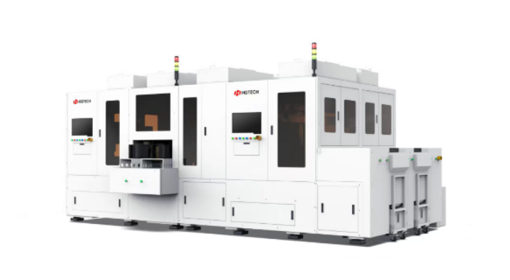
Designed for wafer-level precision manufacturing of key AR optical components, including:
• Geometric optical waveguides
• Diffractive optical waveguides
• Surface relief gratings
• Volume holographic gratings
The fully automated production line integrates:
• Automatic loading
• Laser marking and code reading
• Laser cutting and wafer separation
• AOI inspection
Core Advantages:
HGLaser’s proprietary LCO technology reduces edge chipping from ≥50 μm to <20 μm, improving cutting yield to over 99% while reducing overall production costs by more than 30%.
The solution enables optical waveguides to move from prototype development to industrial-scale mass production.

HGLaser focuses on solving real manufacturing challenges faced by customers, addressing the key factors that determine production success — yield, efficiency, reliability, and scalability.
Through the deep integration of laser processing, intelligent inspection, and automation technologies, HGLaser helps customers overcome the barriers between prototypes and mass production, ensuring every manufacturing process meets the demands of high-volume production.
Looking ahead, HGLaser will continue pushing the boundaries of laser processing technology and accelerating the integration of AI with intelligent manufacturing.
In the upcoming series, HGLaser will further explore the technological innovations and industry applications behind these solutions, demonstrating how advanced manufacturing technologies empower the AI ecosystem — from computing infrastructure and high-speed data transmission to next-generation edge interaction technologies.

