PCB & Microelectronics Industry

Precision laser processing for PCB and microelectronics

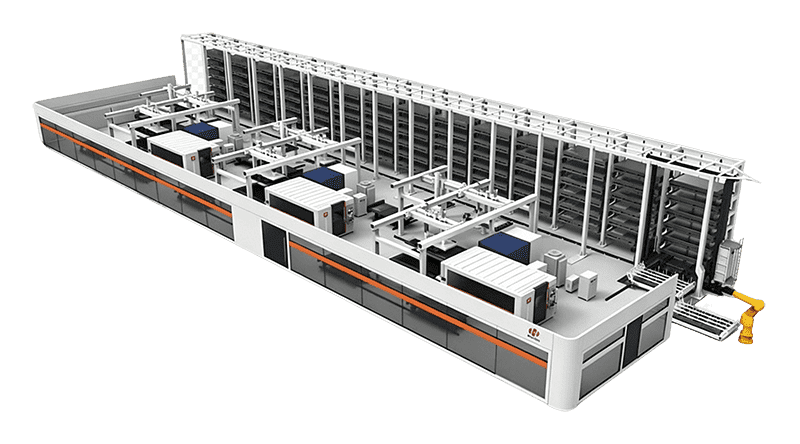
HGTECH provides PCB and microelectronics laser solutions covering PCBA depaneling, PCB/FPC marking, FPC drilling, FPC cover film cutting, ceramic substrate cutting, IC substrate X-Out marking, IC package marking, inspection support, automation integration, and traceability management.

  • 01

    PCBA Depaneling

    High-precision laser cutting for PCBA production lines.
  • 02

    PCB/FPC Marking

    Coding, reading detection, and traceability for PCB and FPC boards.
  • 03

    FPC Drilling

    High-speed micro-hole drilling for FPC and rigid-flex boards.
  • 04

    FPC Cutting

    Cover film cutting, shape cutting, window half cutting, and RFPC cover opening.
  • 05

    IC Substrate & Packaging Marking

    X-Out marking, IC surface marking, OCR inspection, and MES data feedback.
  • 06

    Ceramic Substrate Cutting

    Automatic cutting for alumina, zirconium oxide, aluminum nitride, silicon nitride, and related ceramic substrates.

Core Equipment

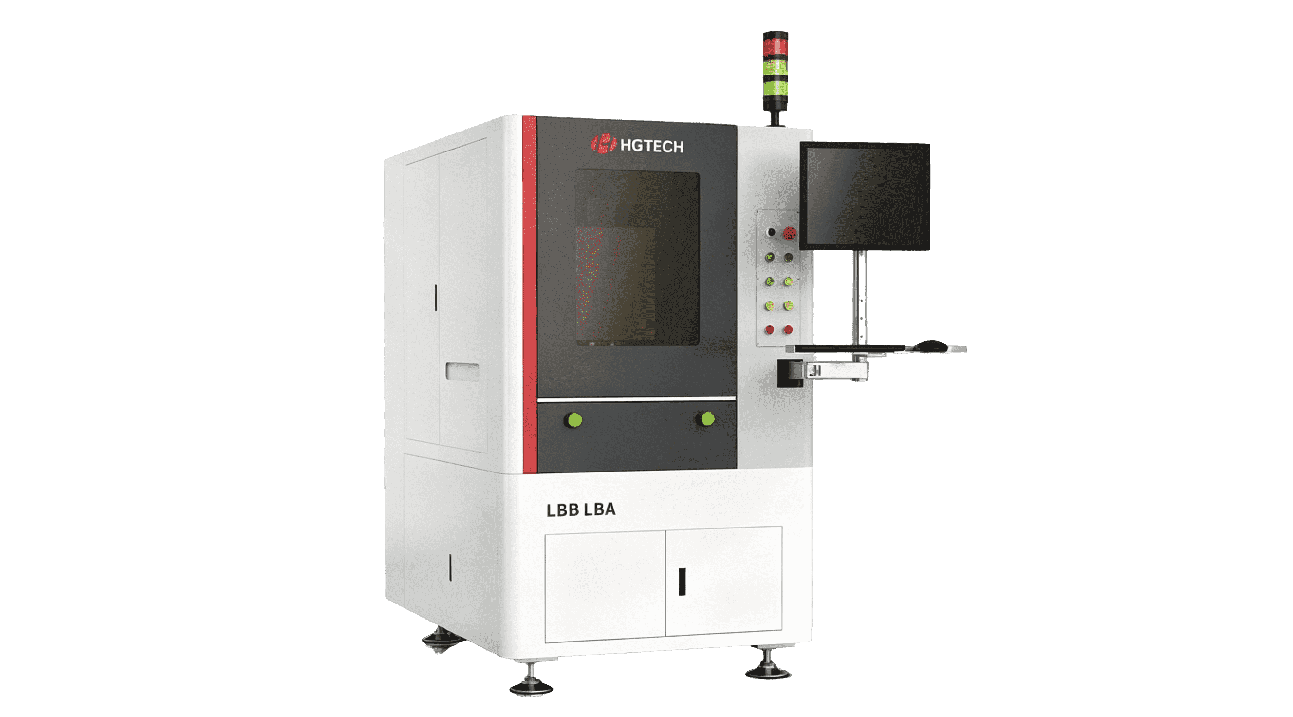
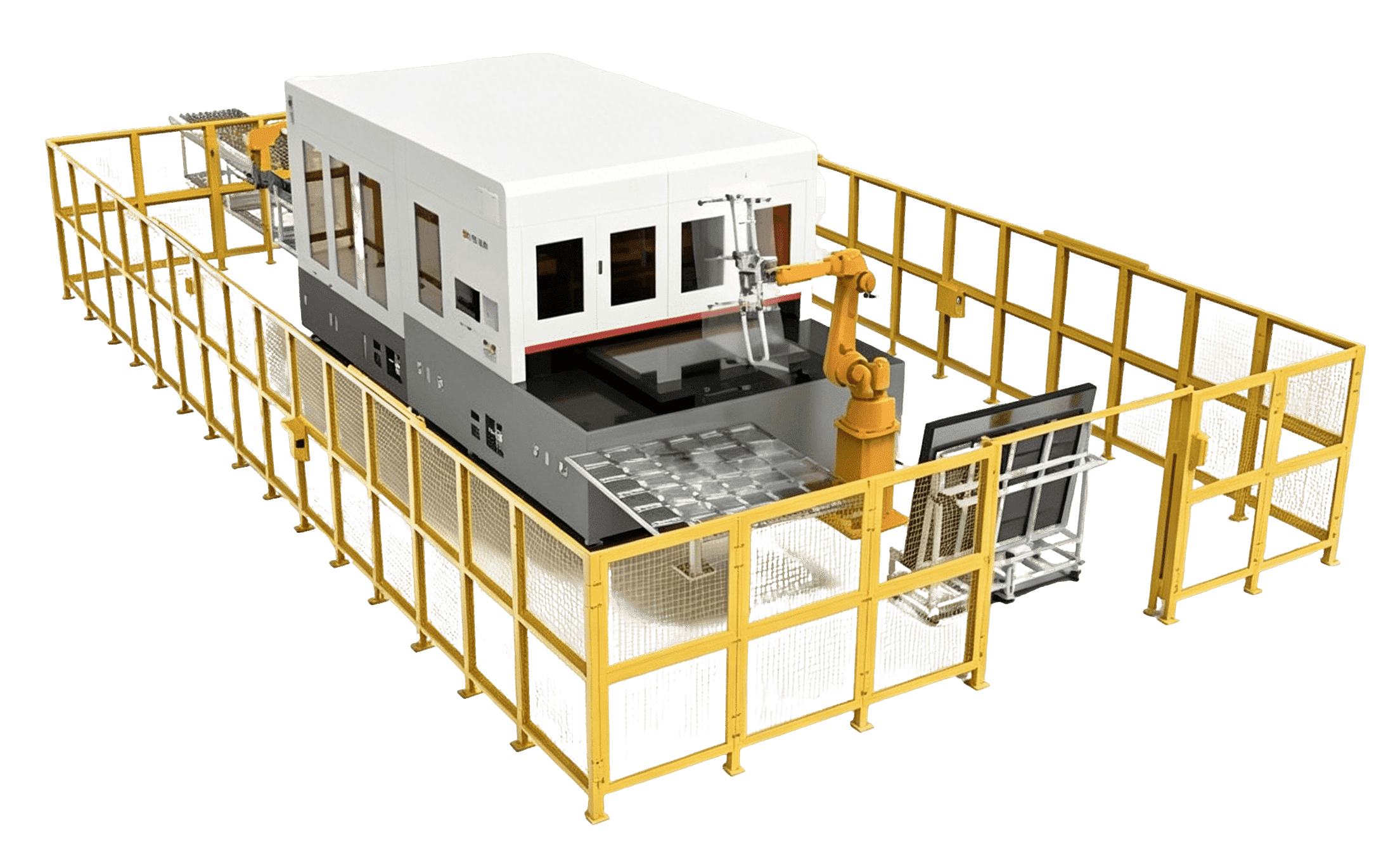
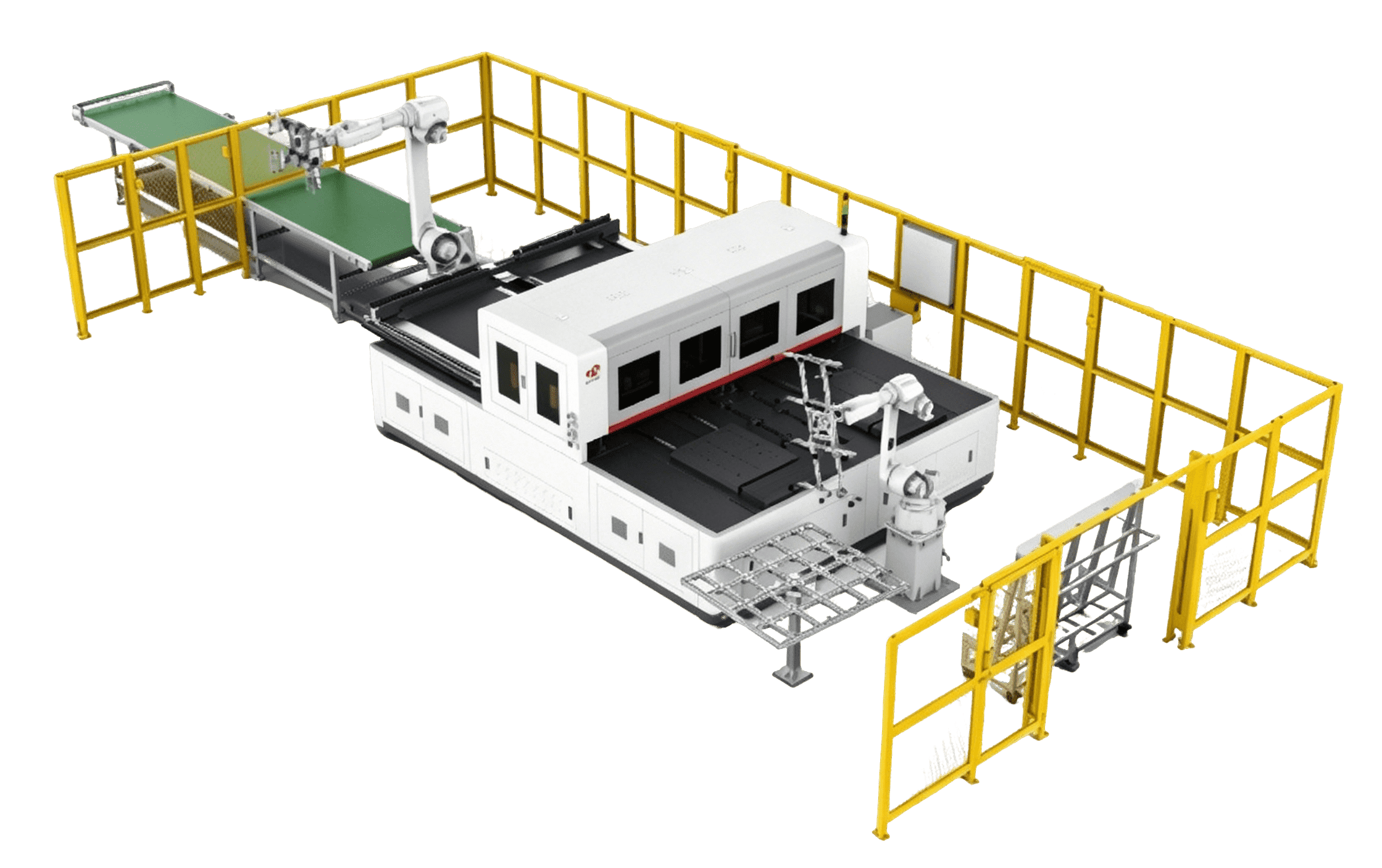
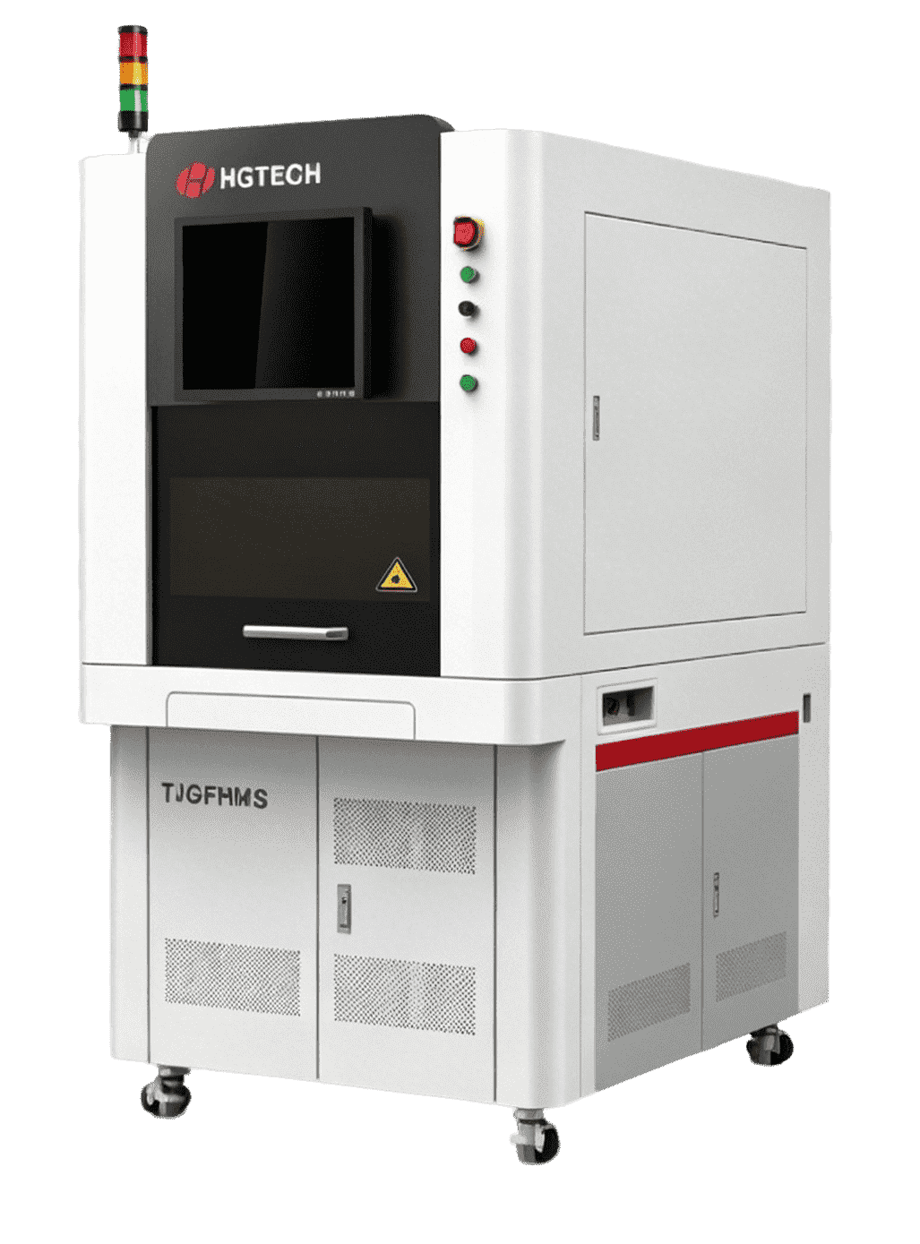
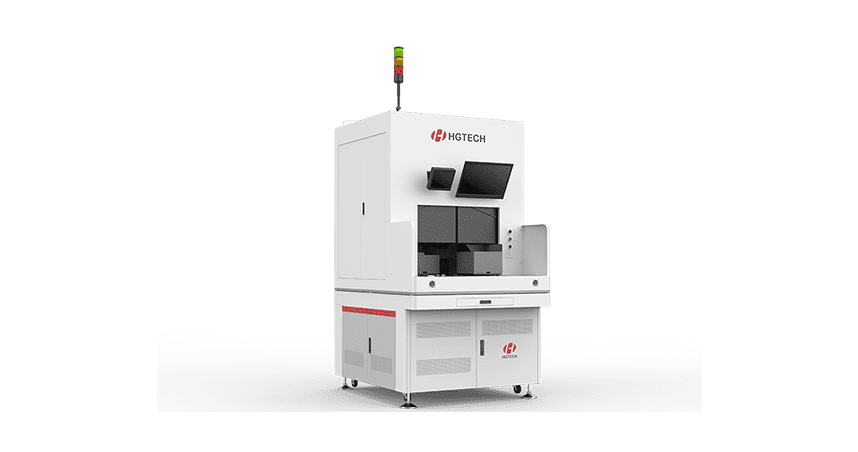
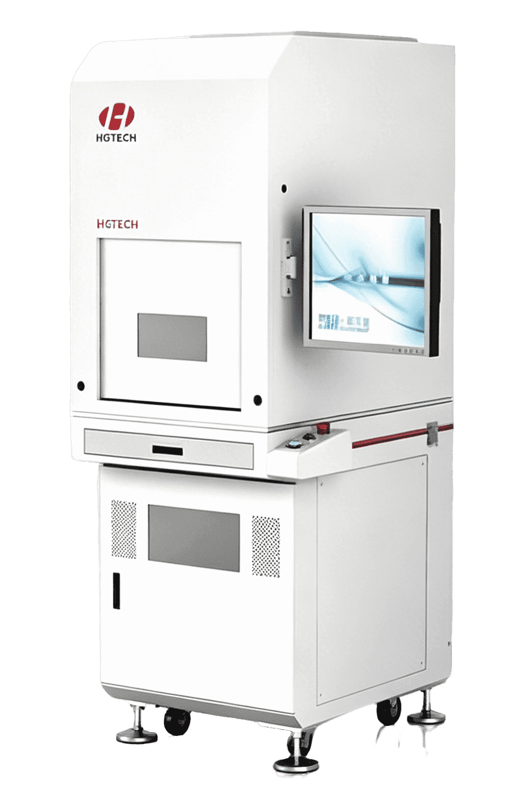
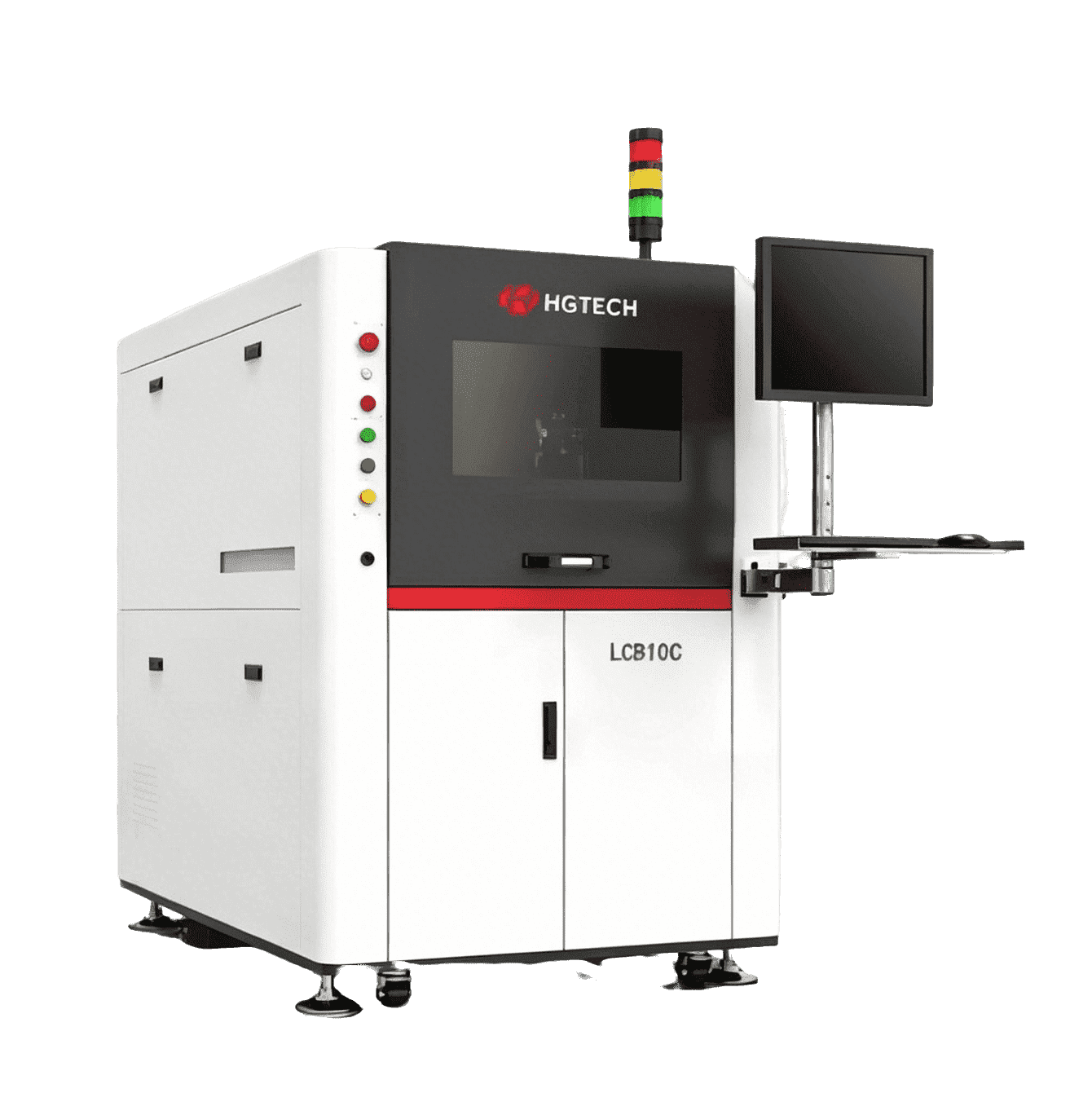
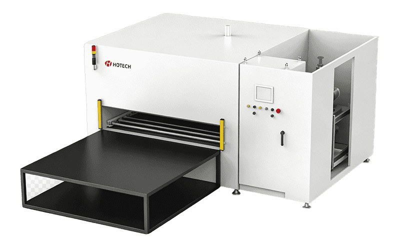
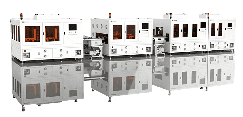
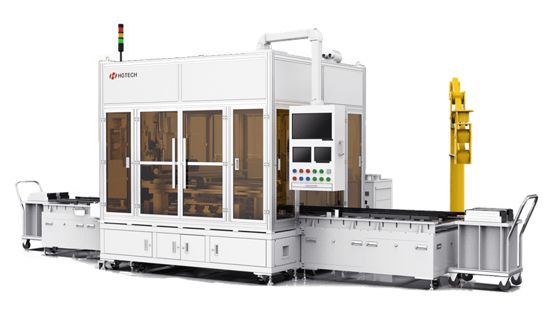
  • SMT Laser Depaneling

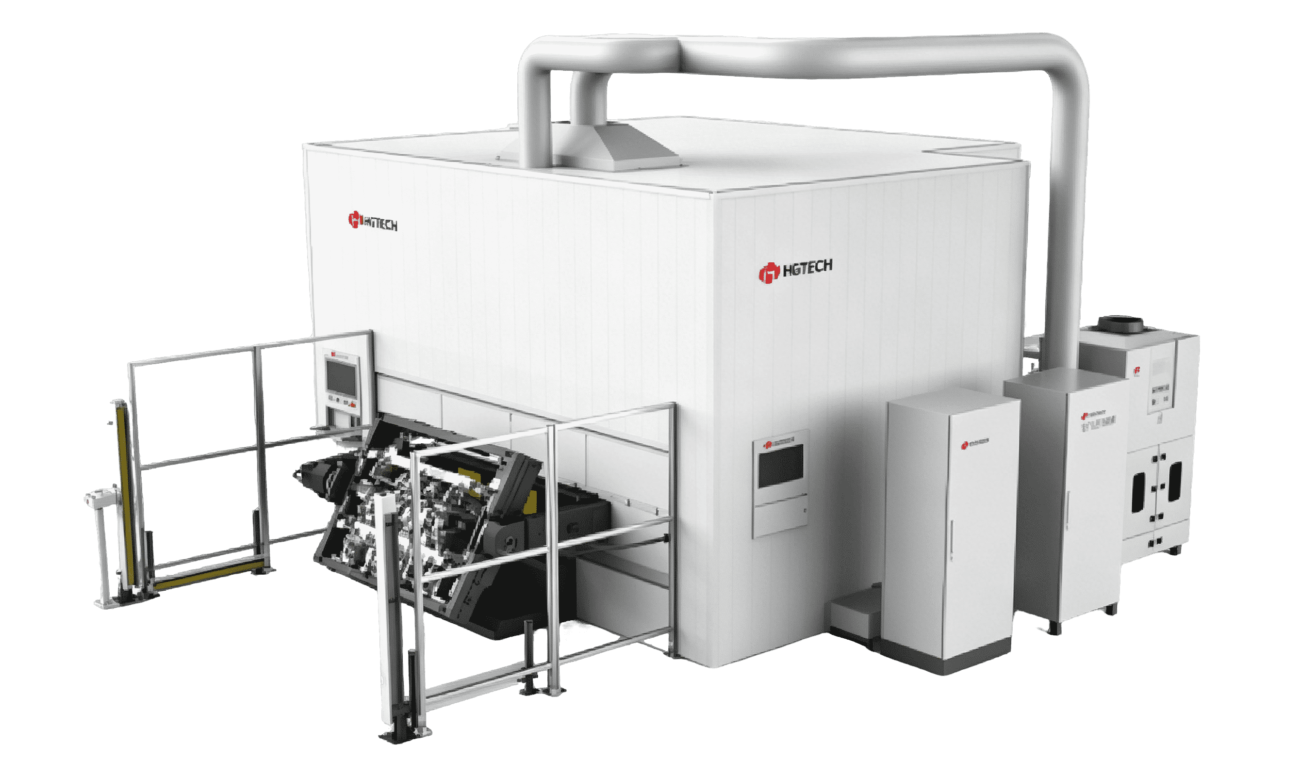
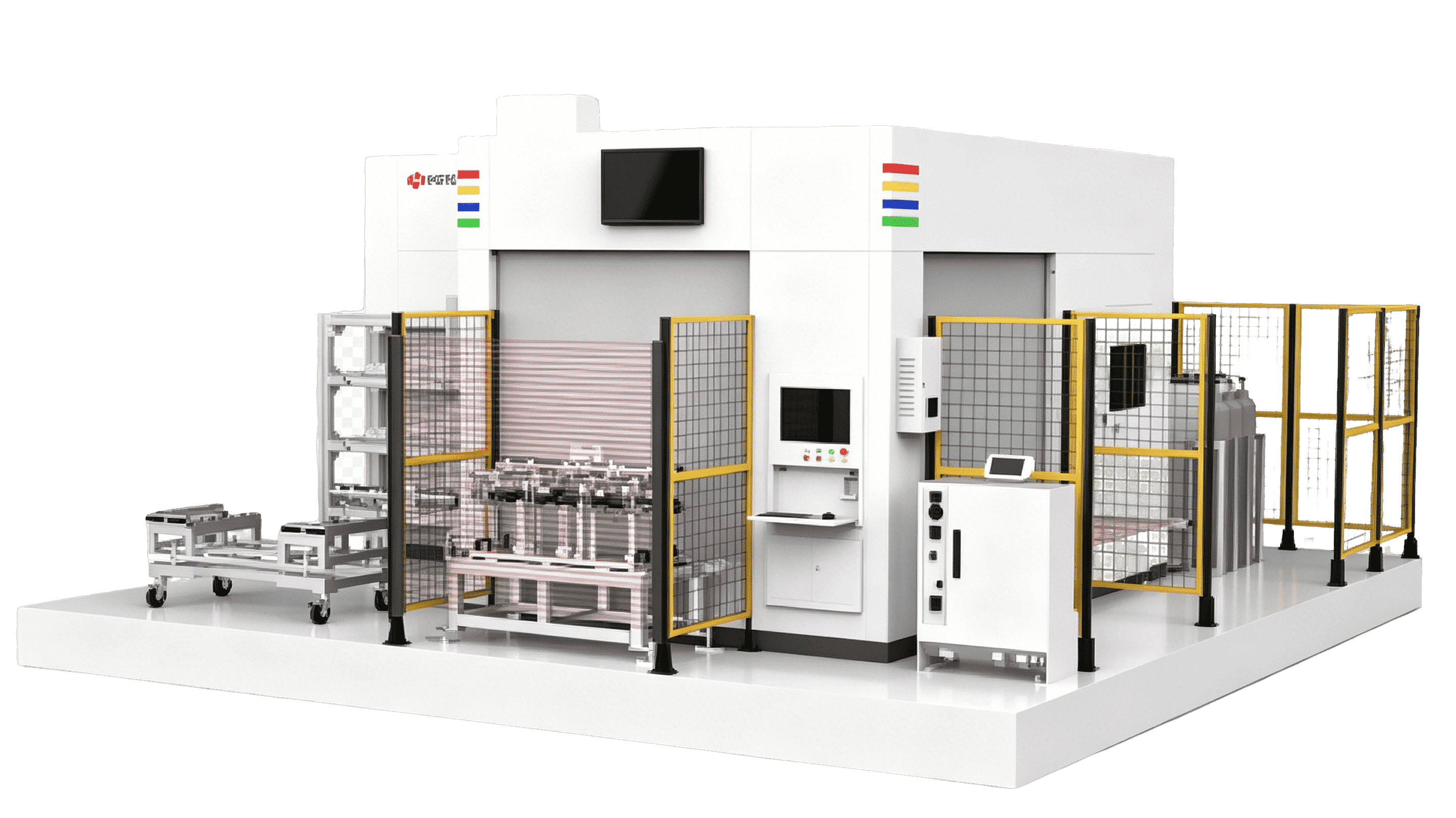
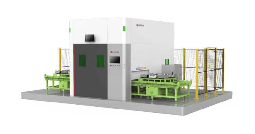
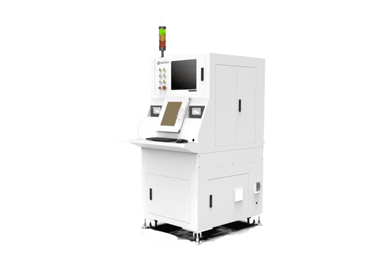
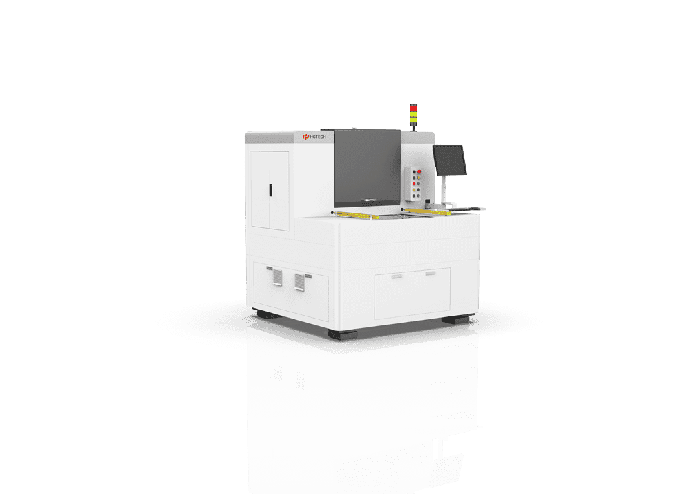
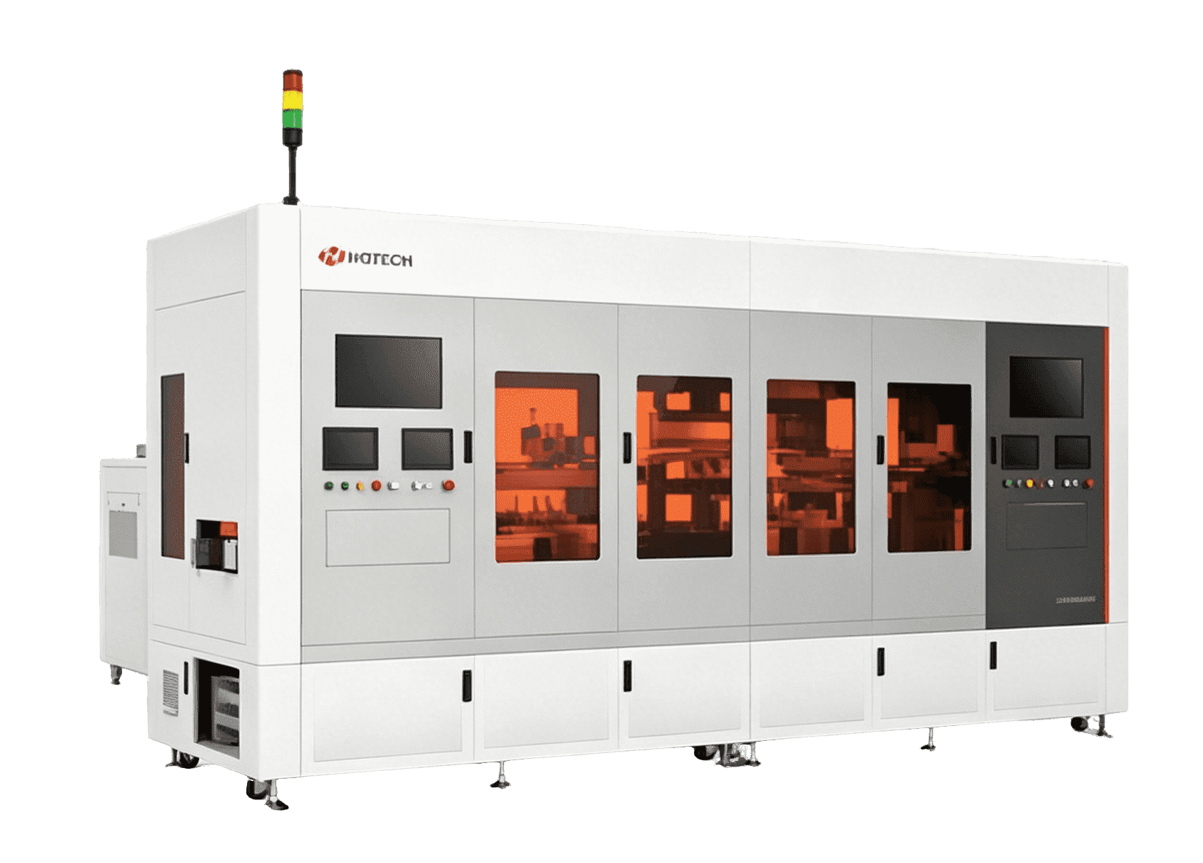
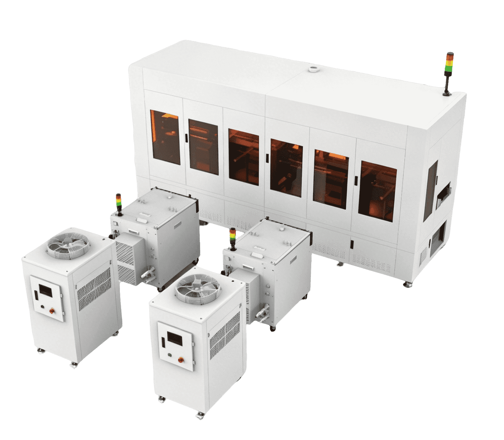
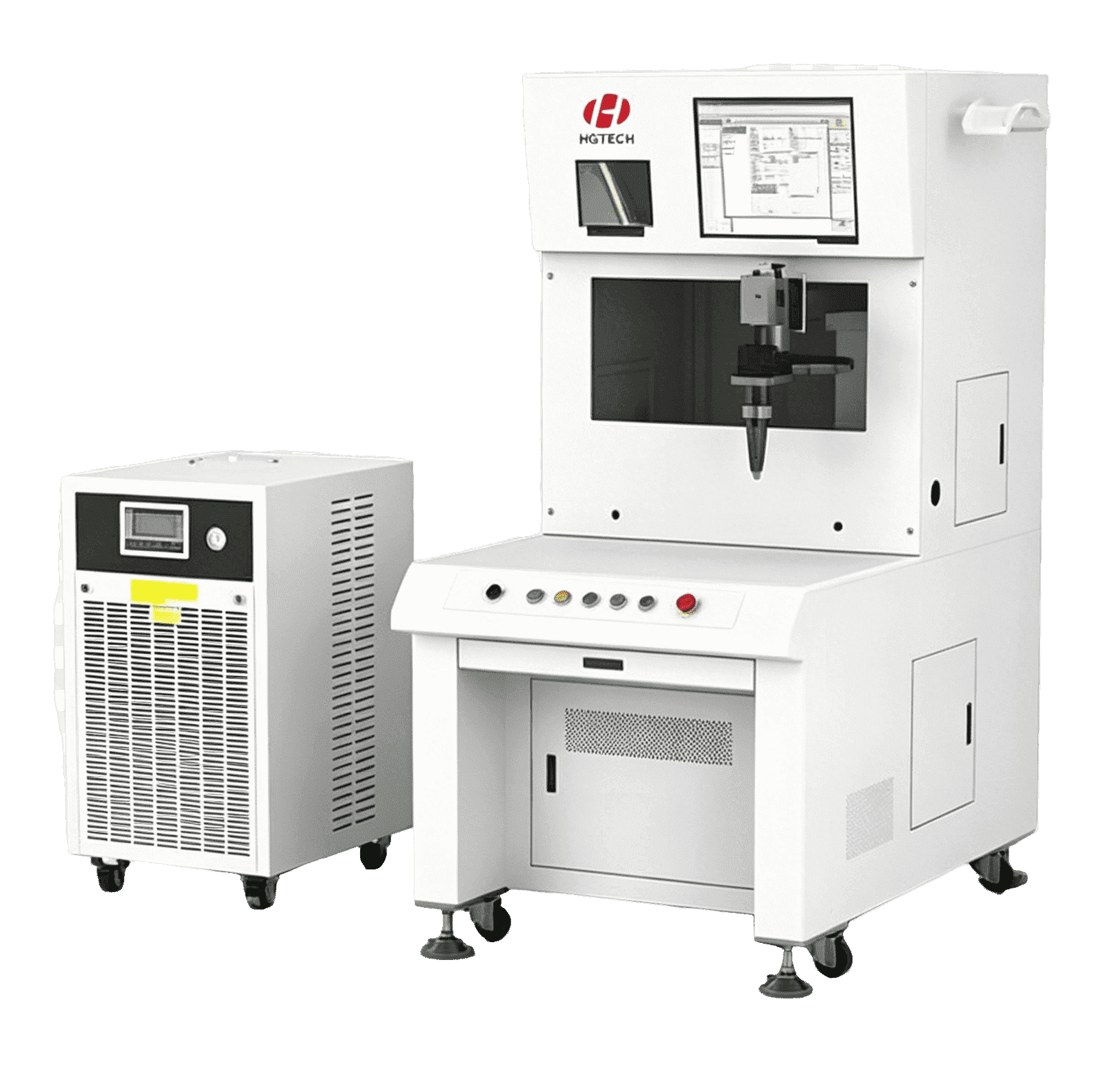
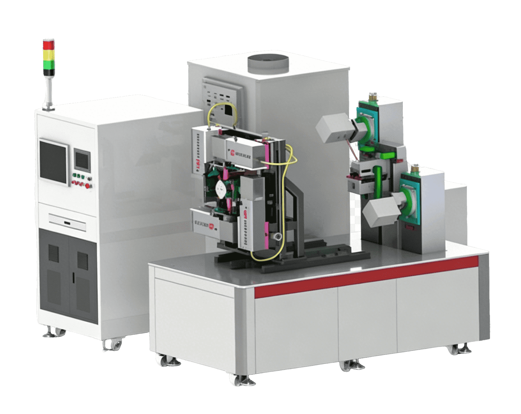
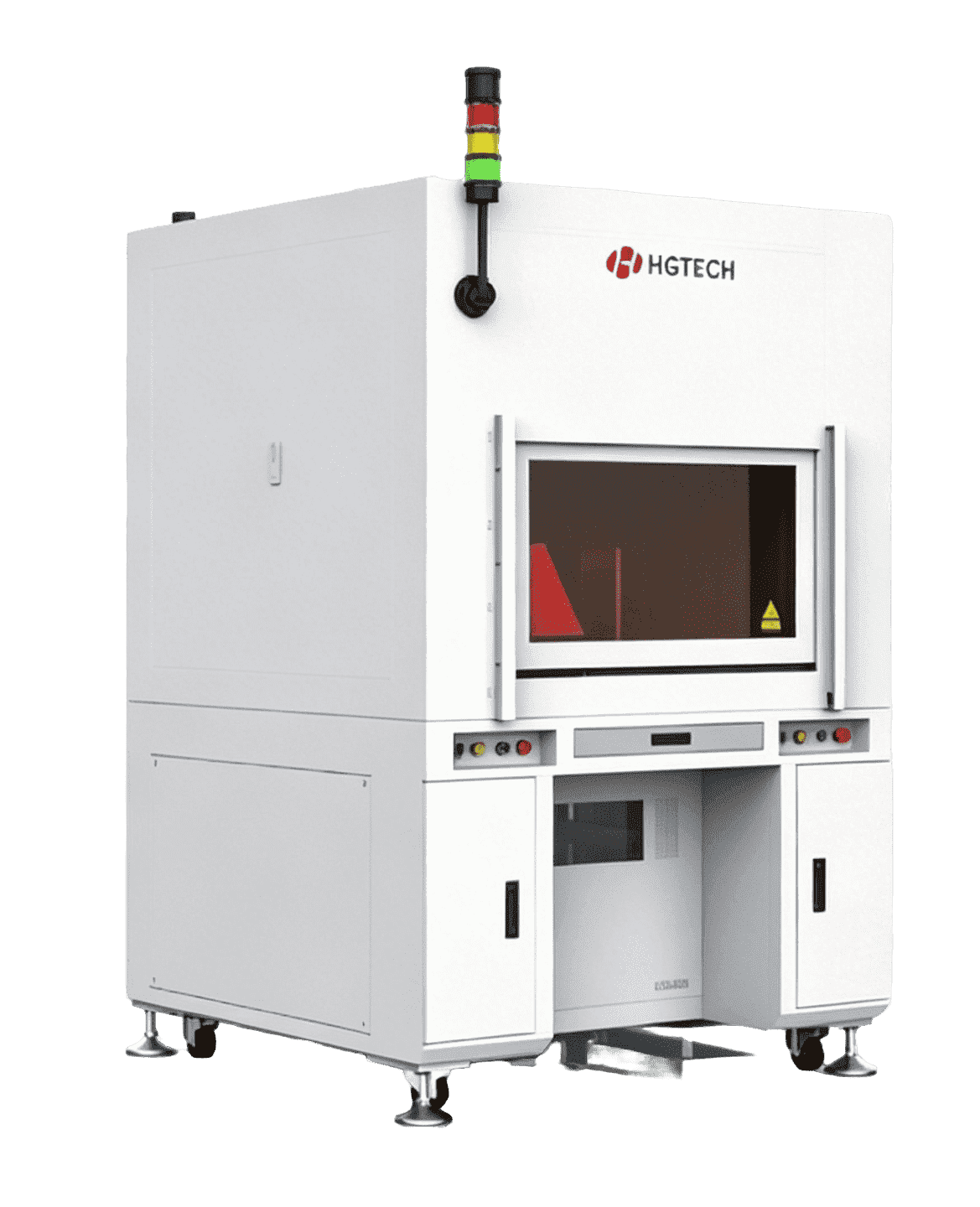
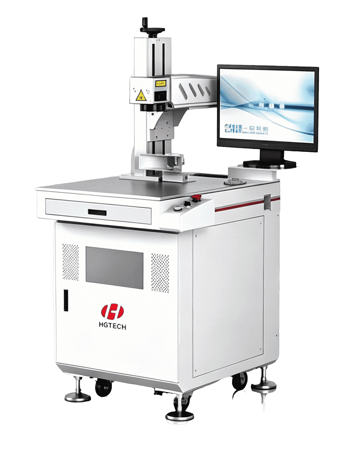
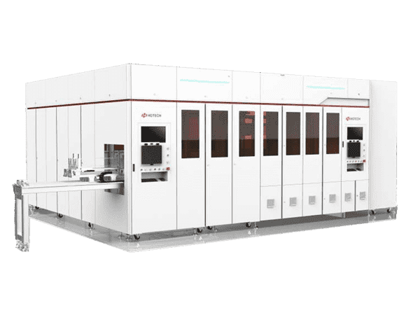
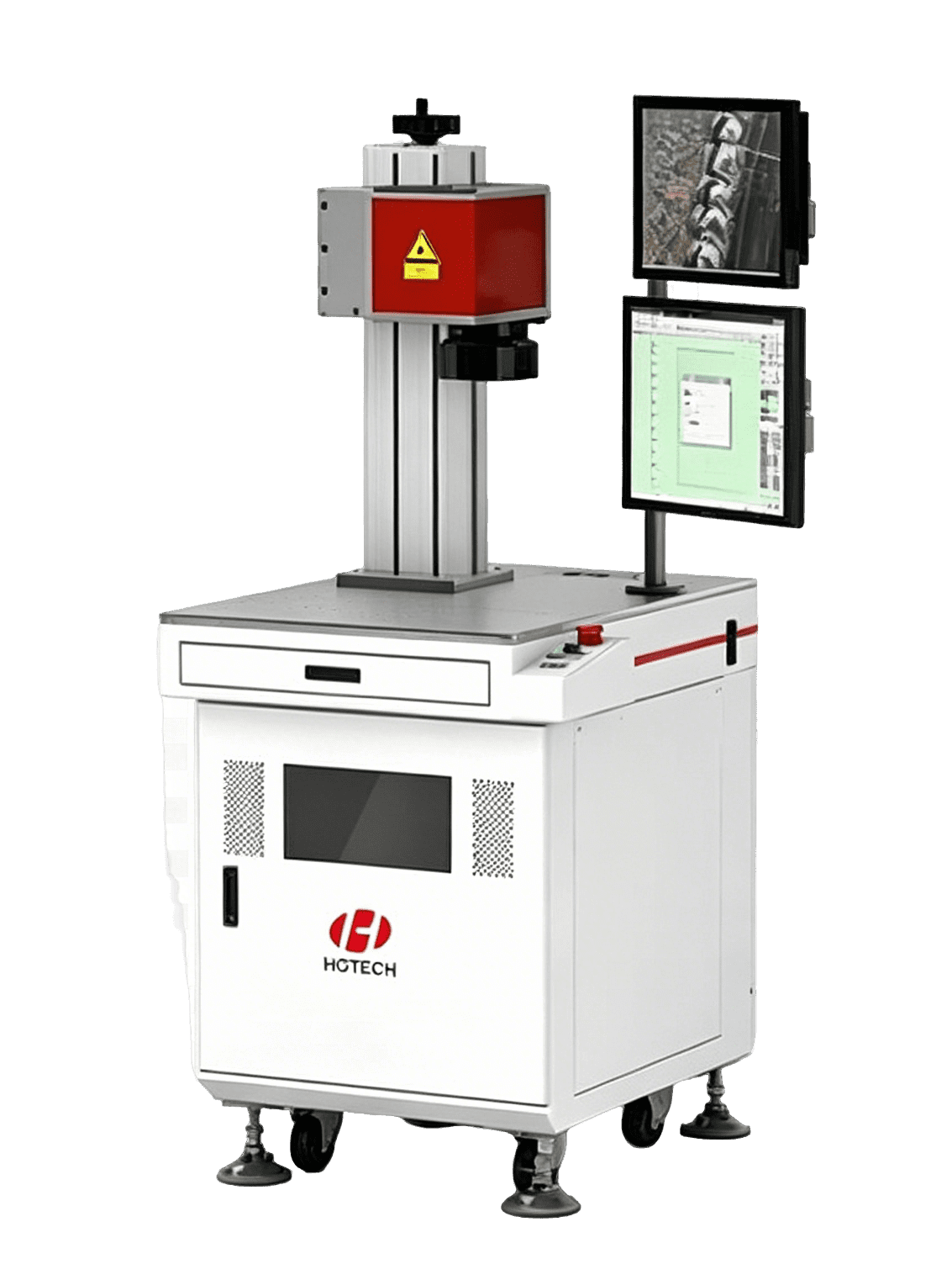
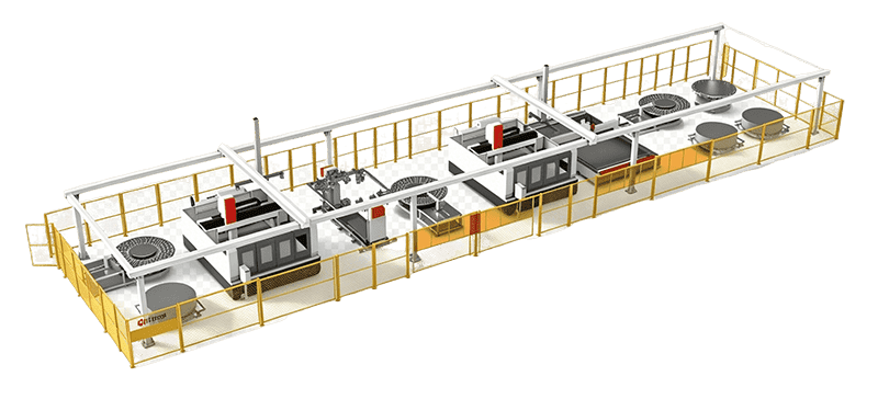
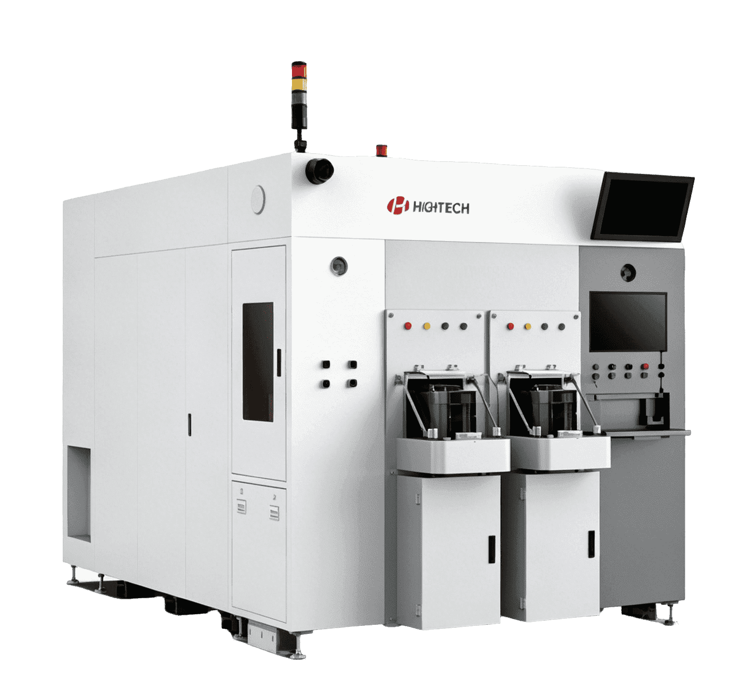
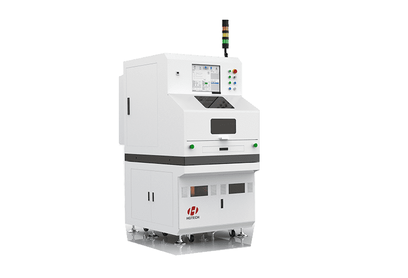
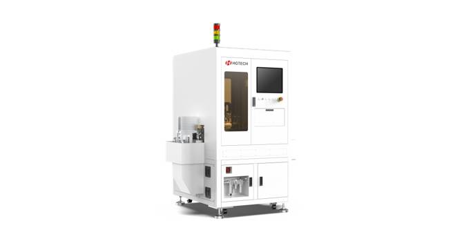
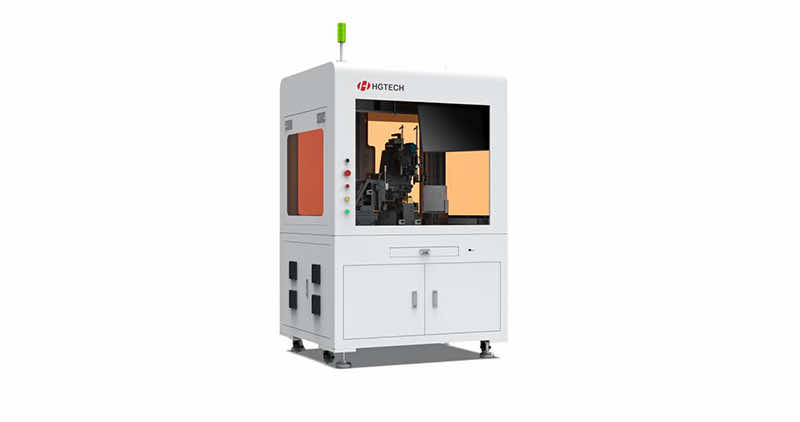
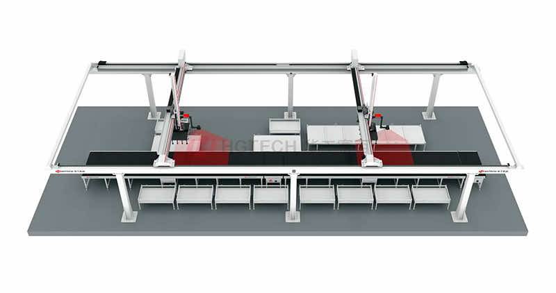
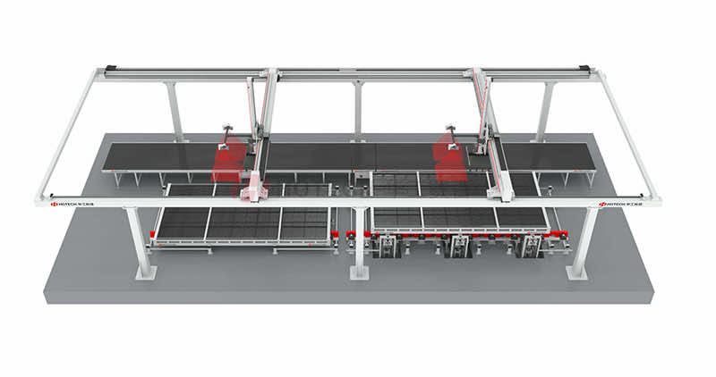
    SMT laser depaneling solutions support PCBA production lines with offline or inline configurations and fully automatic laser cutting through high-precision control and industrial vision systems.
    Value Points
    No dust and deformation | Suitable for PCBA production lines | MES data interoperability
    Recommended Products
    SMT Laser Depaneling Machine
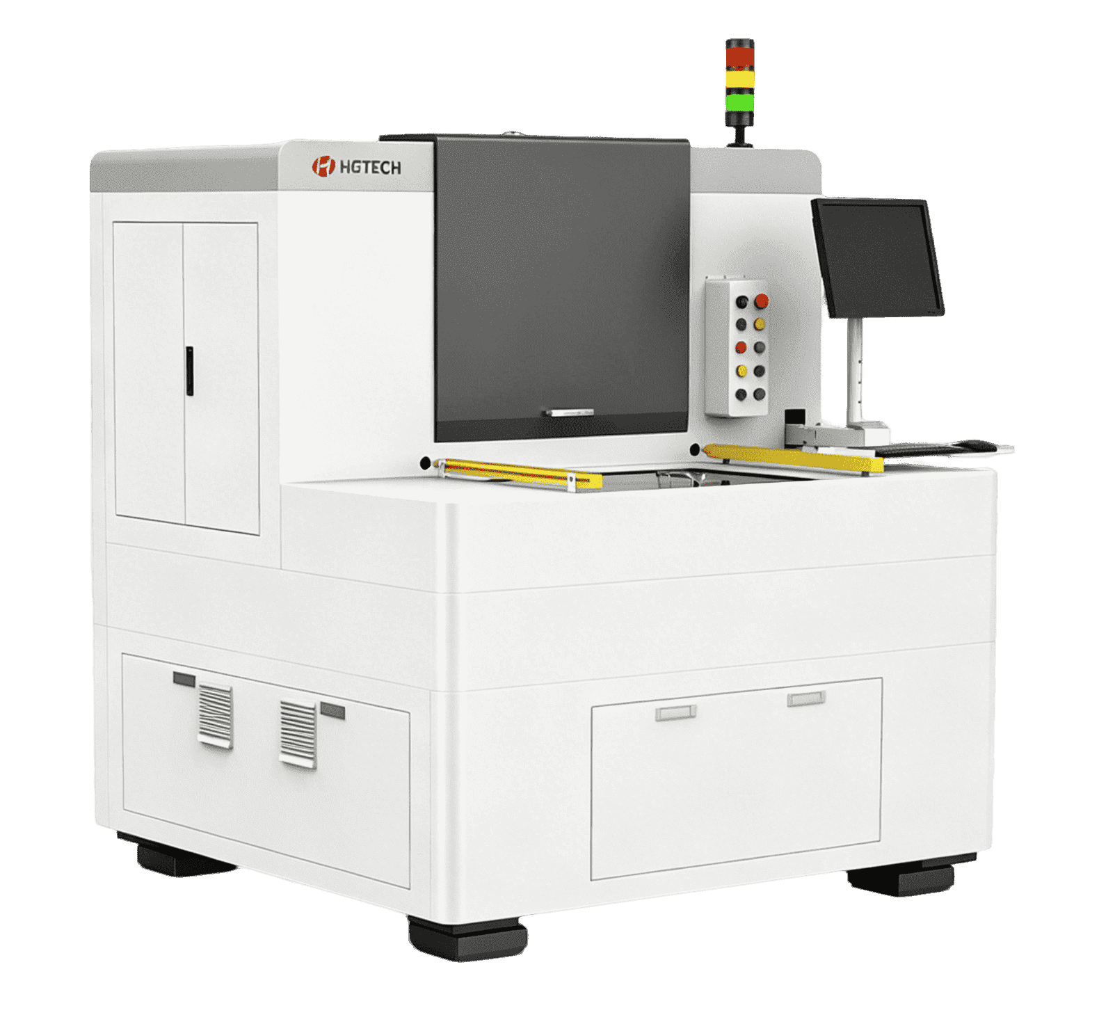
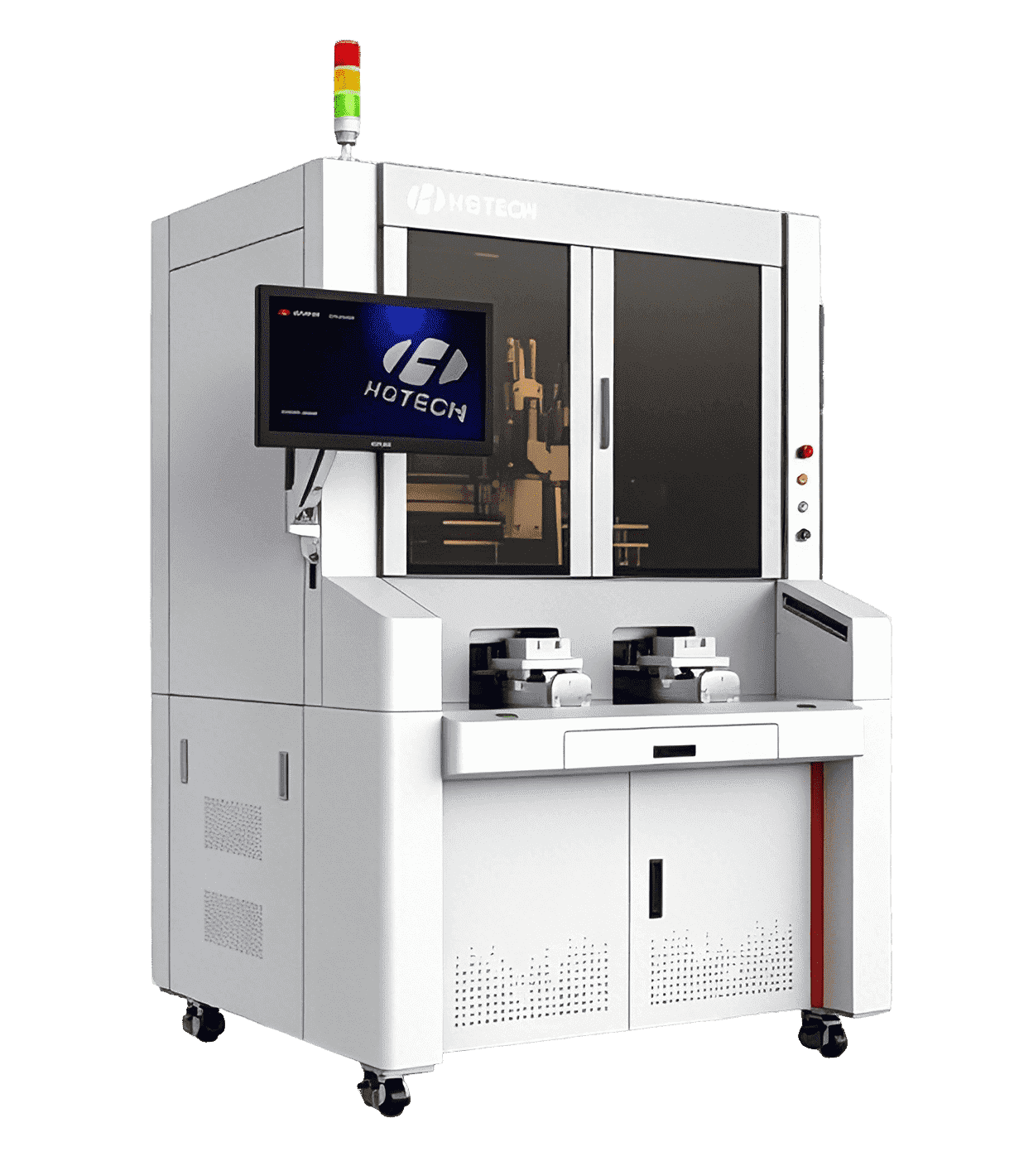
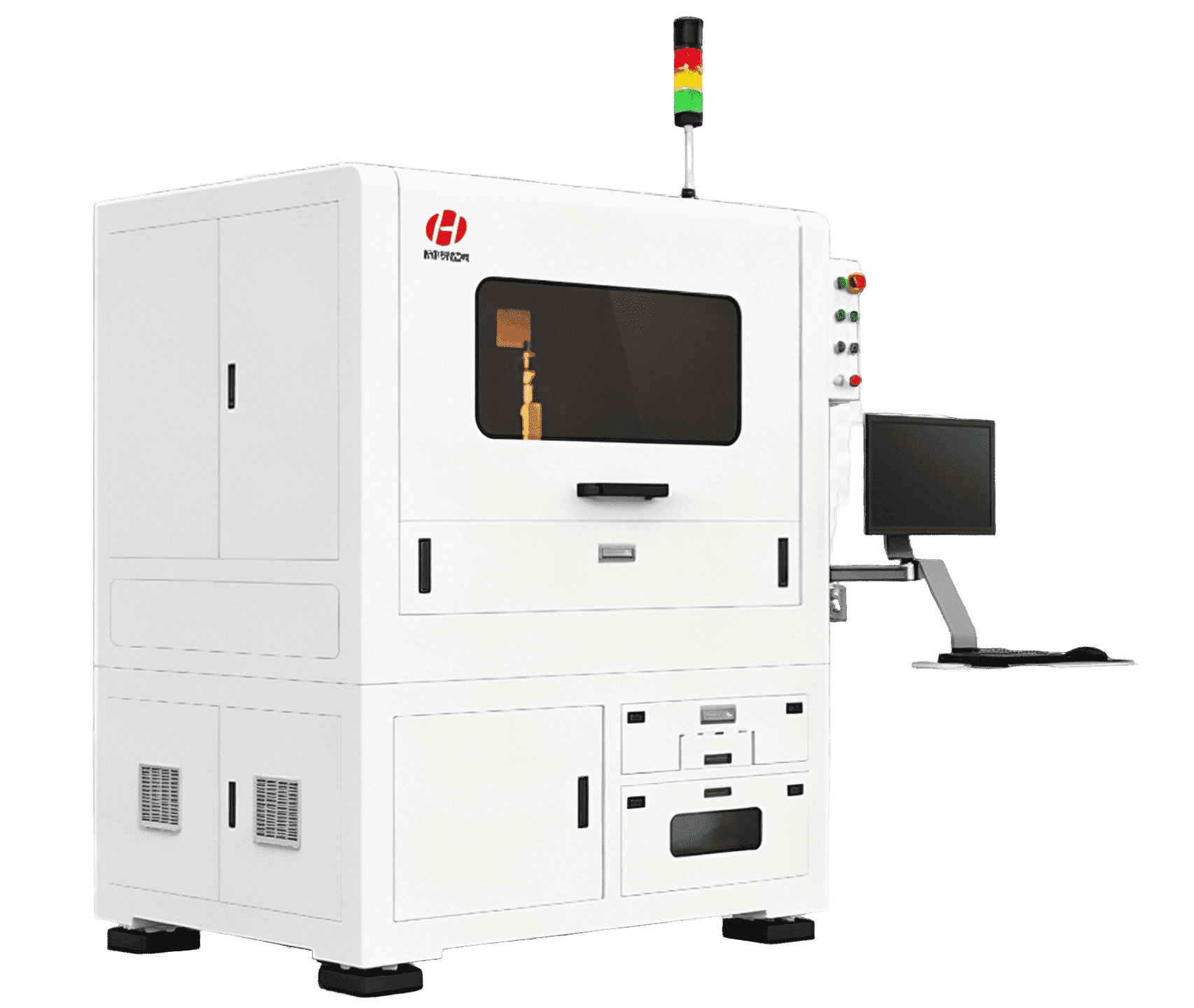
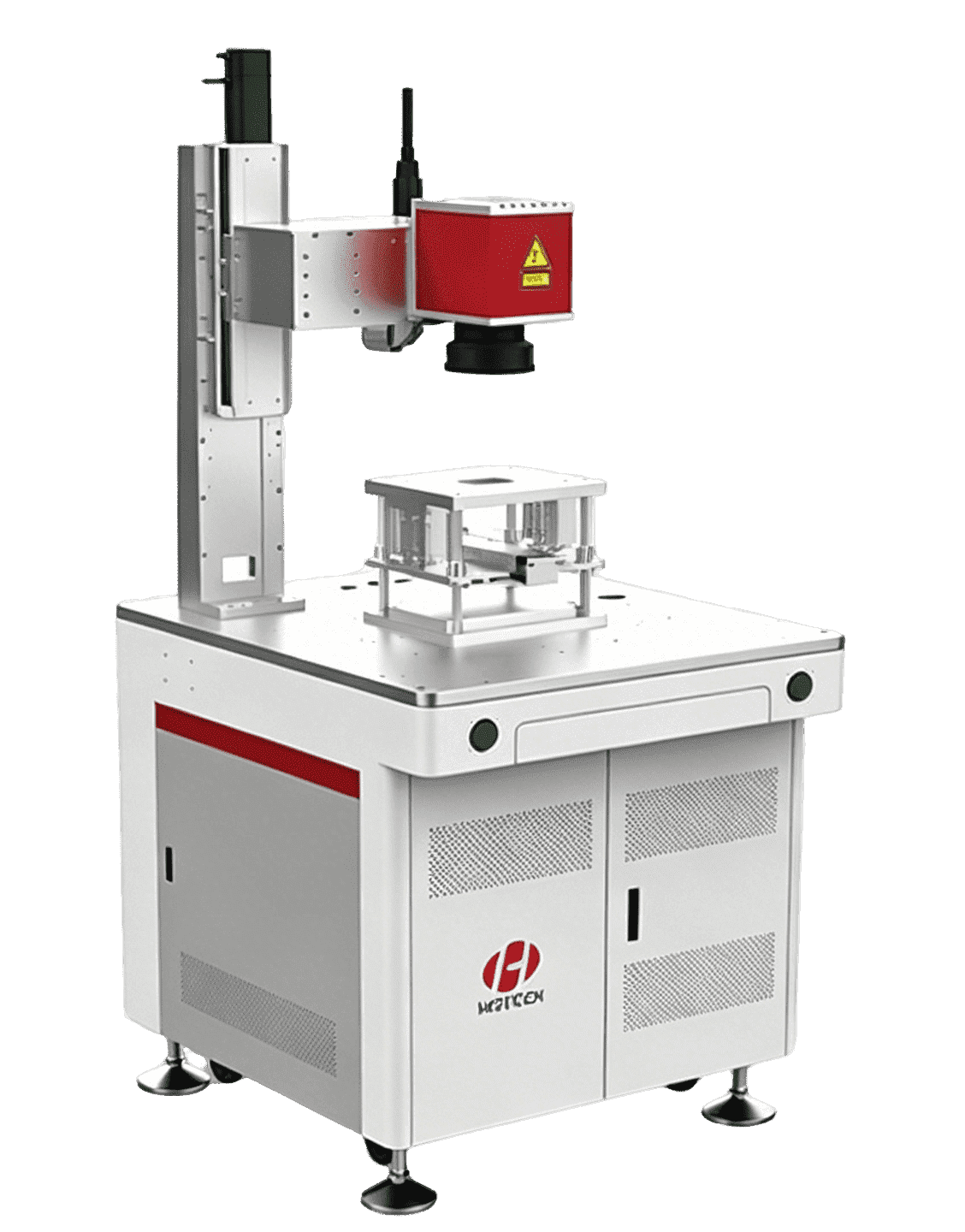
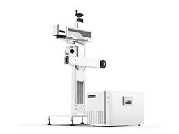
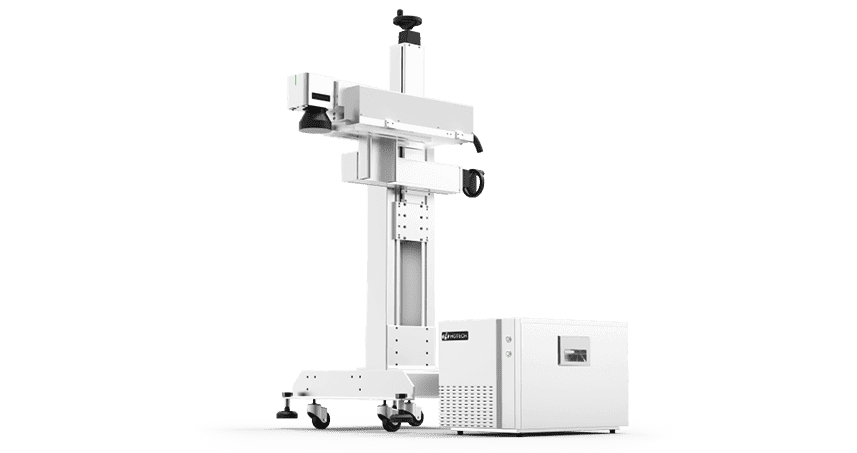
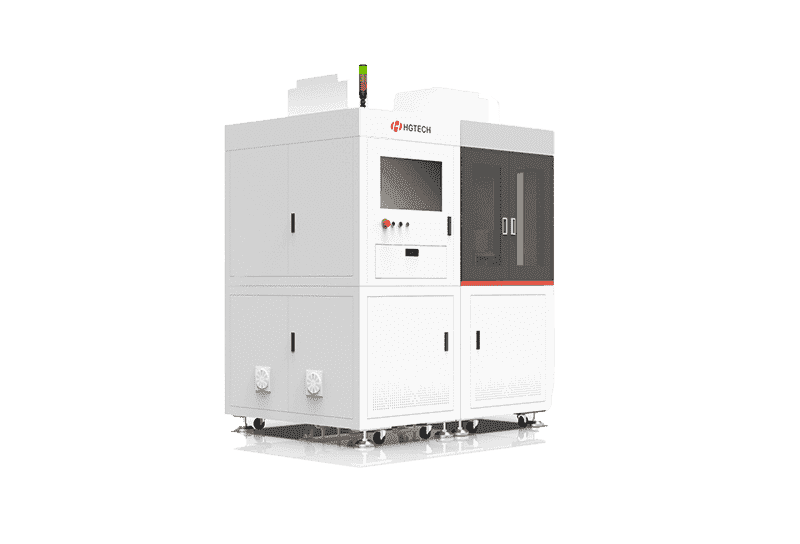
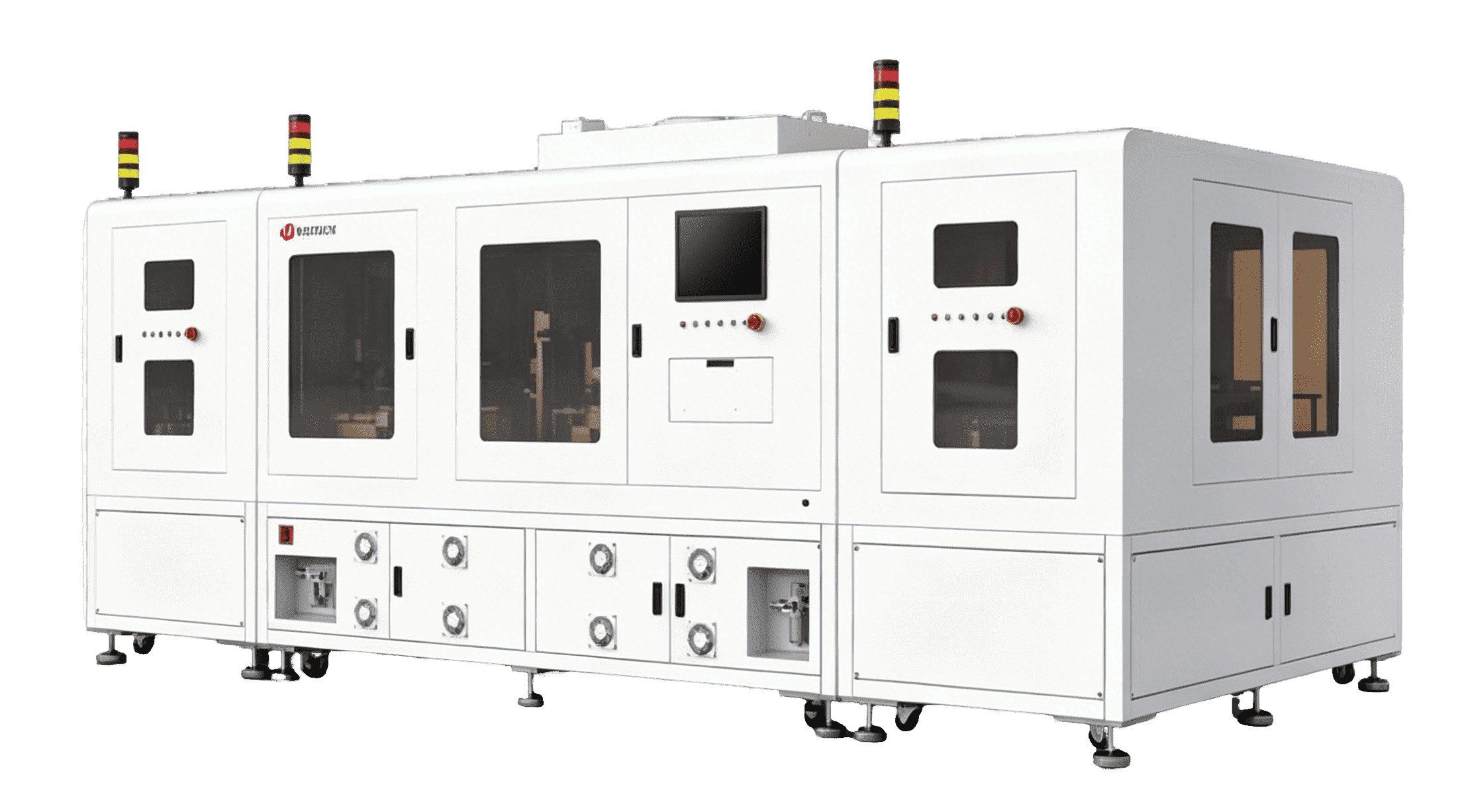
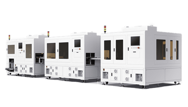
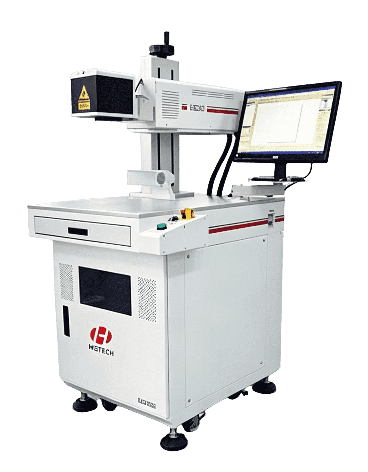
  • SMT Double Head PCB Laser Marking

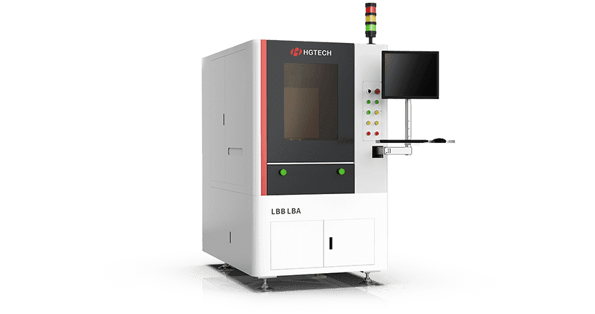
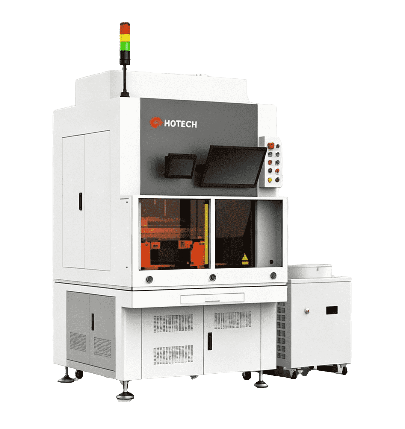
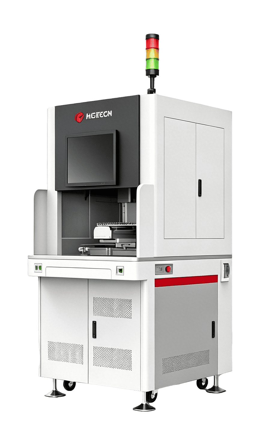
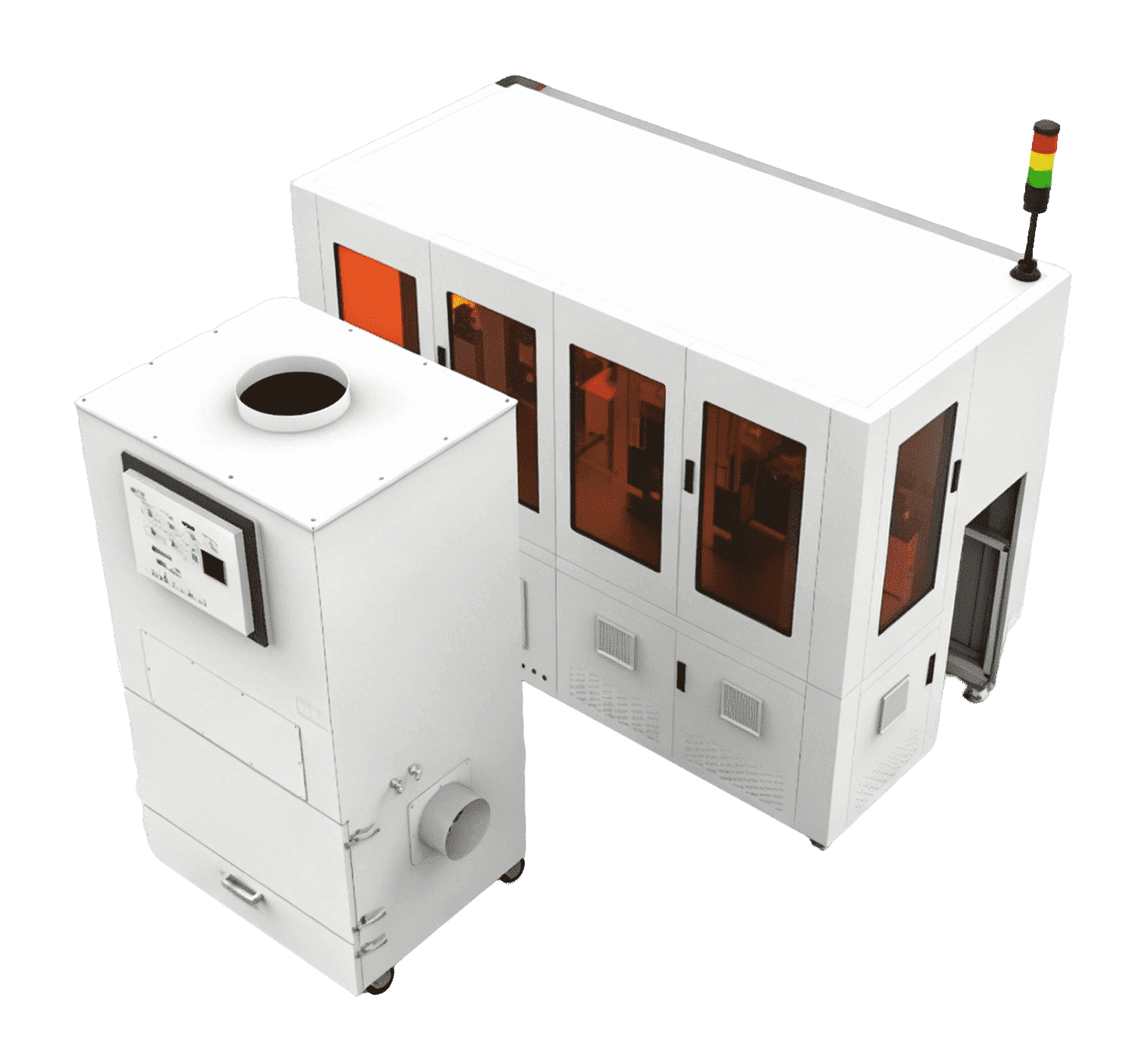
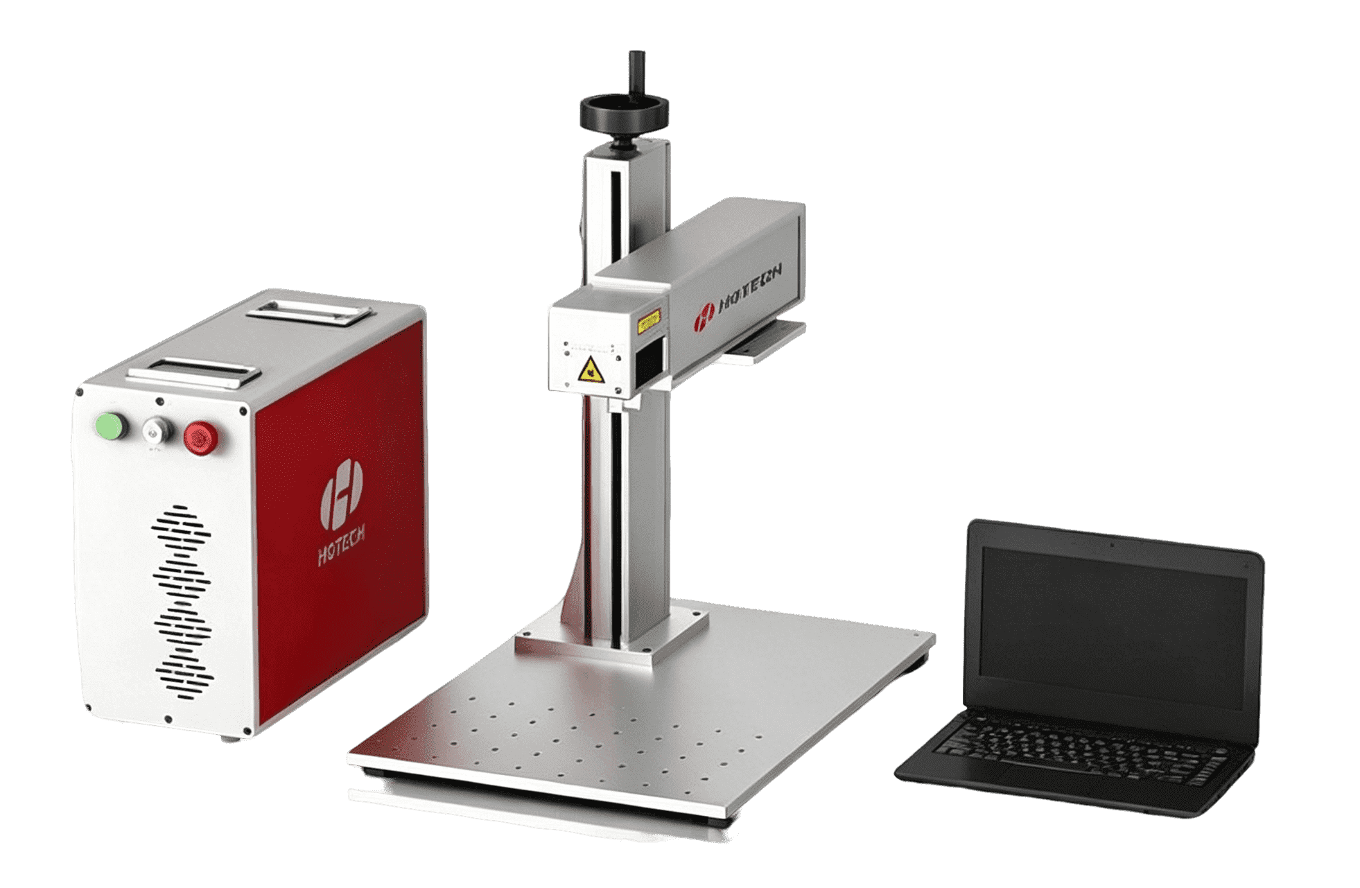
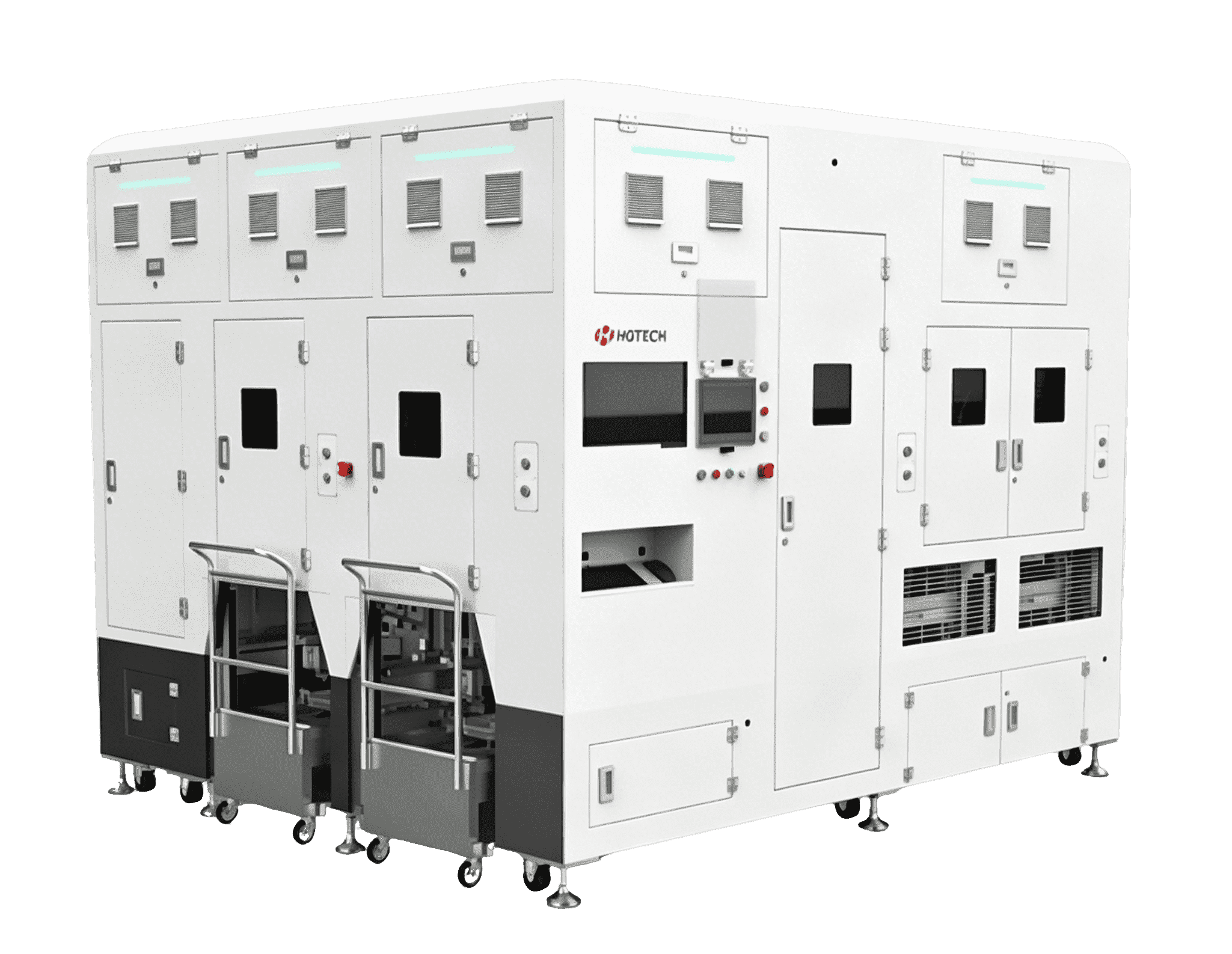
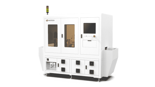
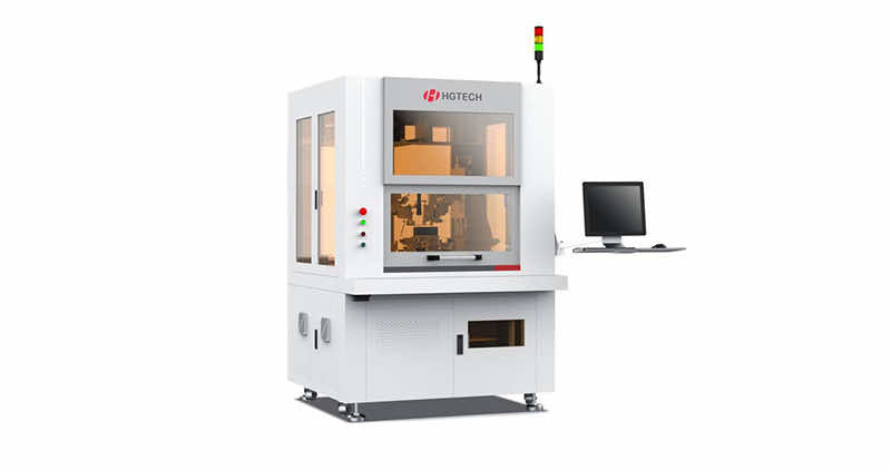
    SMT double-head PCB laser marking solutions support automatic laser coding, reading detection, and process control for PCBA production lines.
    Value Points
    Supports one-dimensional and two-dimensional codes | Compatible with PCB/FPC materials and metal shielding covers | MES interconnection and data anti-duplication
    Recommended Products
    SMT Double Head PCB Laser Marking Machine
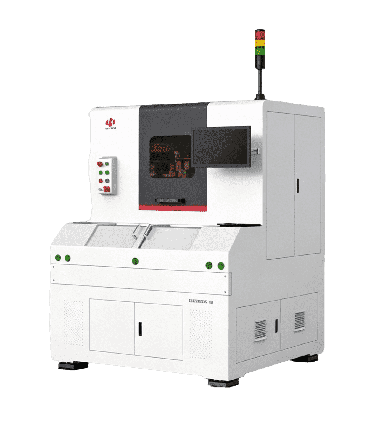
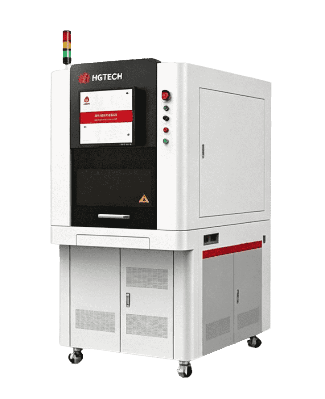
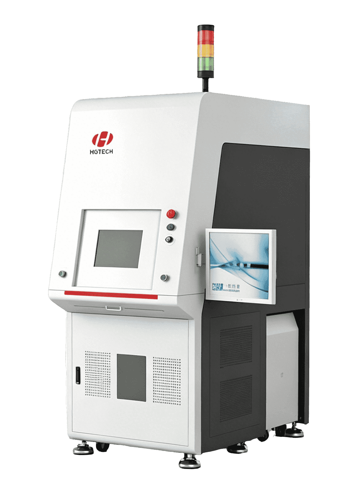
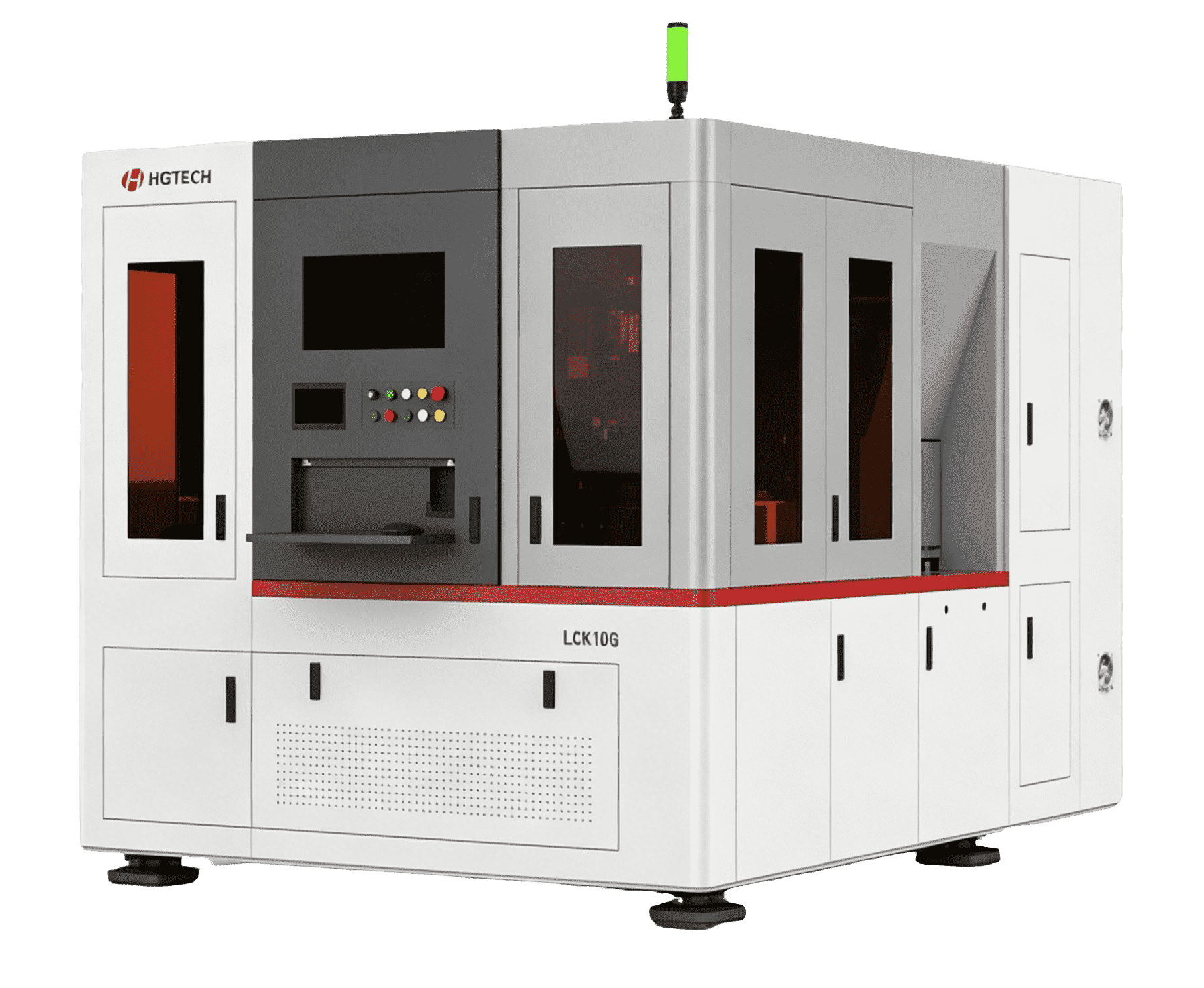
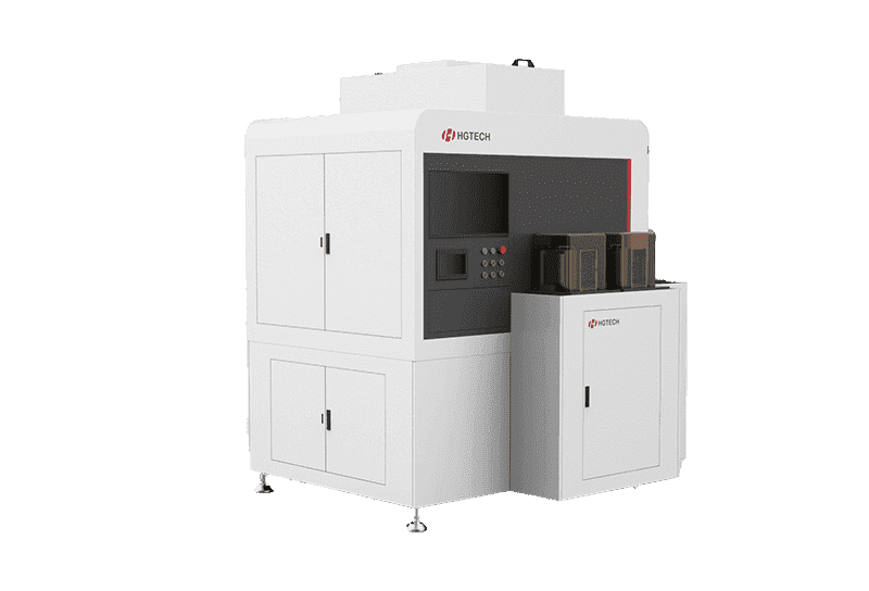
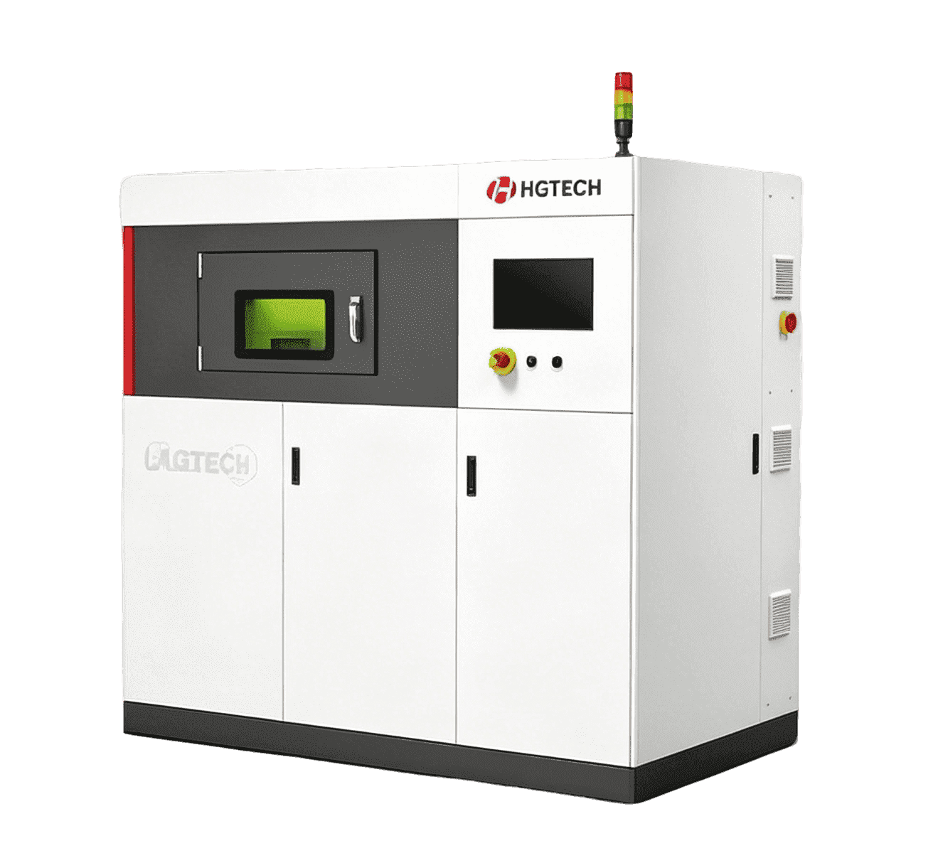
  • IC Substrate X-Out Laser Marking

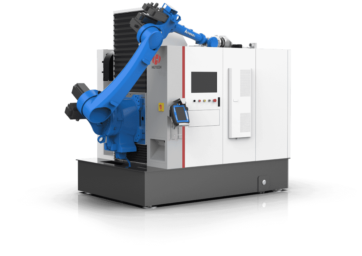
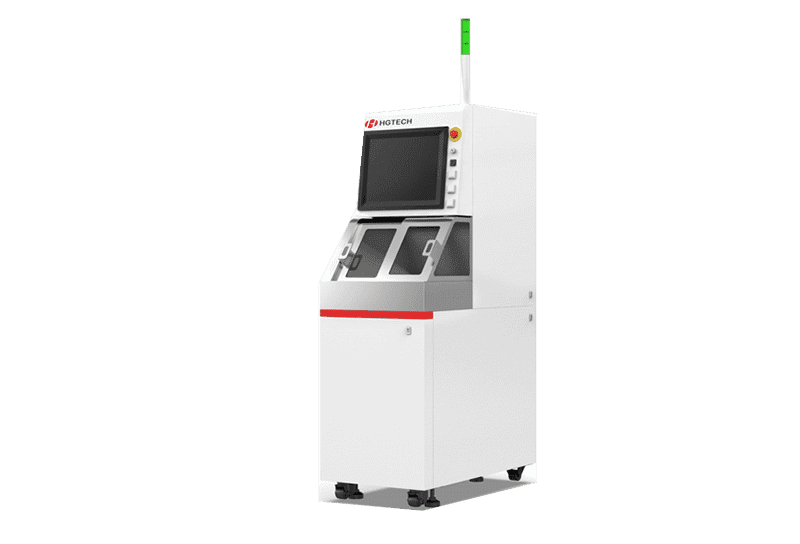
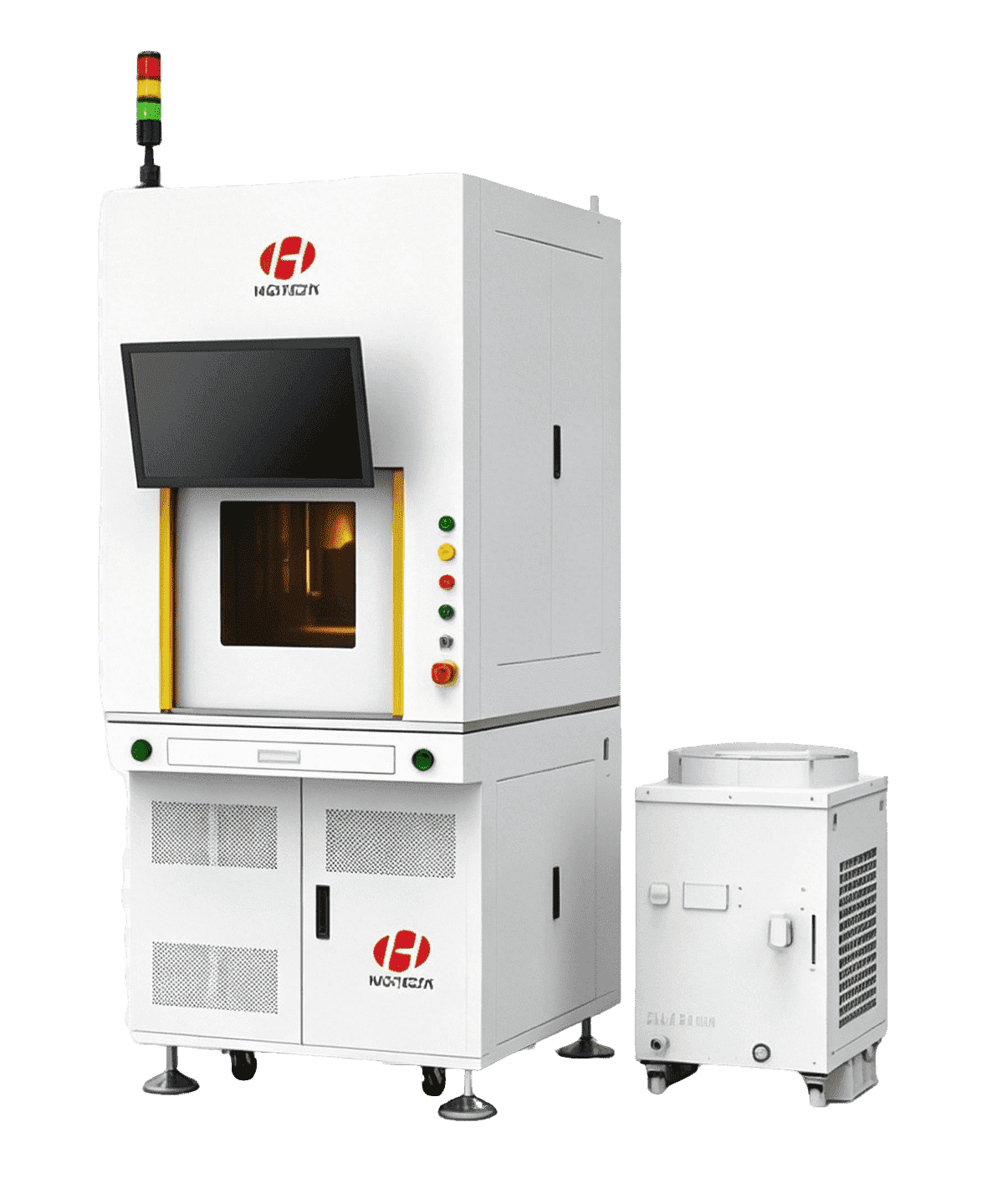
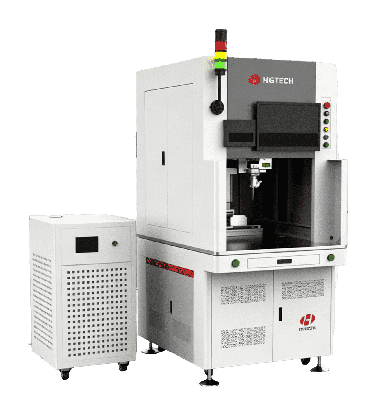
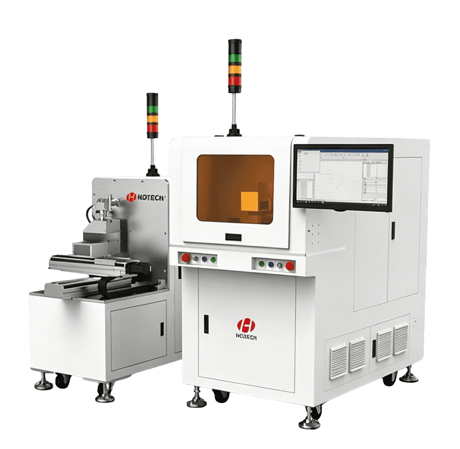
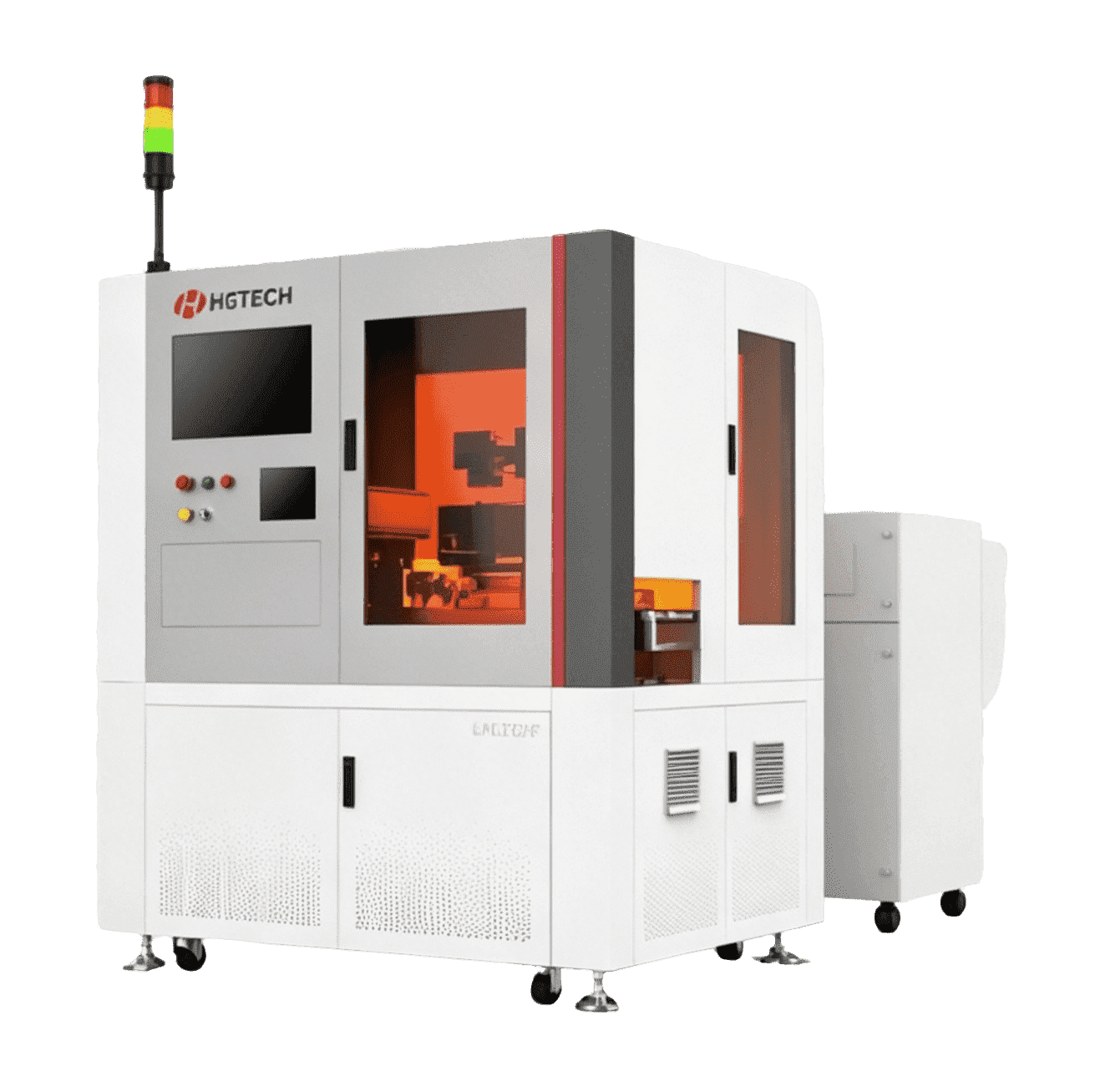
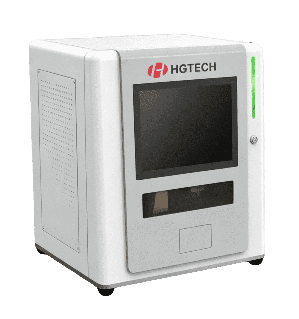
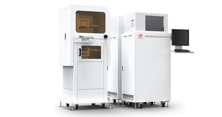
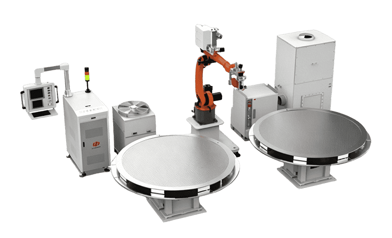
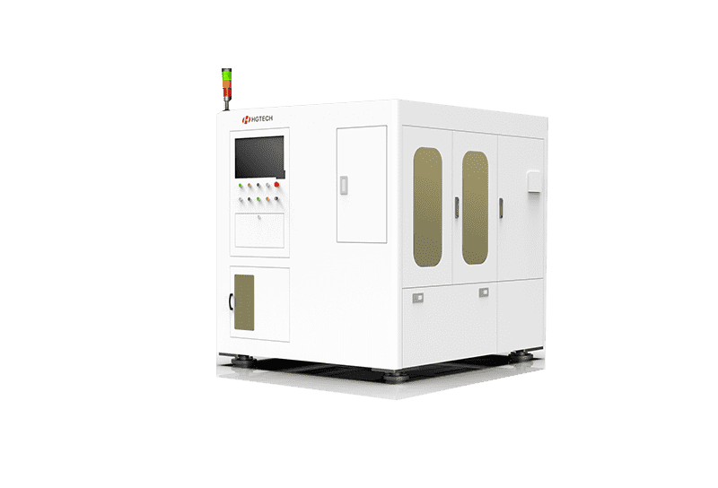
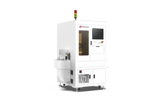
    IC substrate X-Out laser marking solutions are used for automatic identification and laser marking of scrap units on carrier products.
    Value Points
    Supports scrap-unit identification | Improves subsequent process identification | Supports yield and process efficiency improvement
    Recommended Products
    IC Substrate X-Out Laser Marking Machine
  • High-Speed FPC Laser Drilling

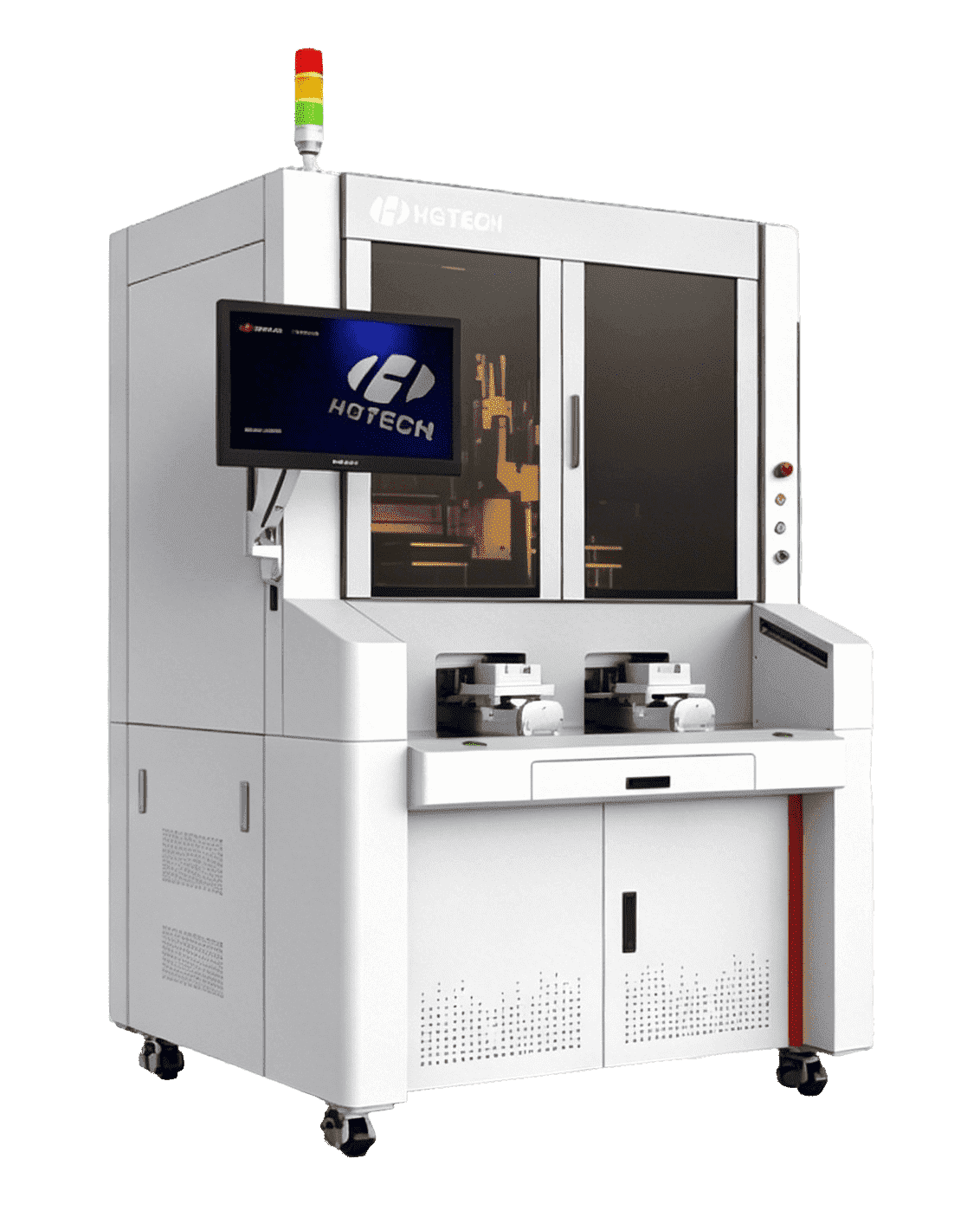
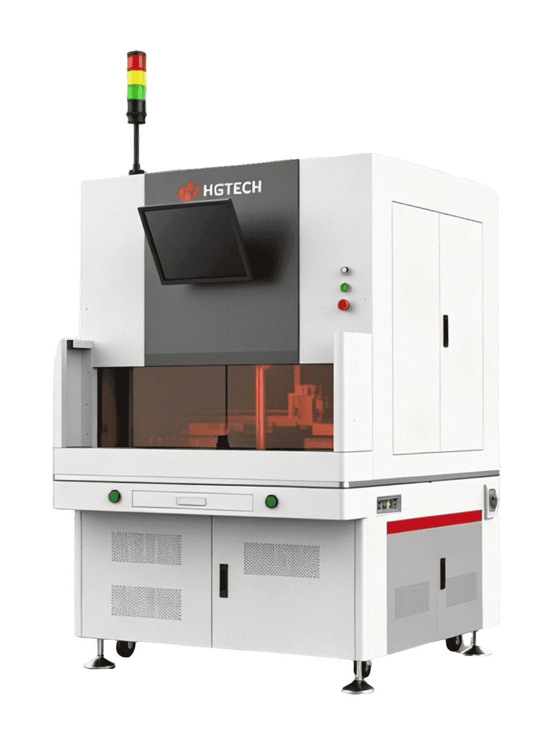
    High-speed FPC laser drilling solutions support high-precision micro-hole drilling for FPC, rigid-flex boards, and related materials.
    Value Points
    High-speed micro-hole processing | Supports blind holes in one hit | Suitable for FPC shape and cover film processing
    Recommended Products
    High-Speed FPC Laser Drilling Machine
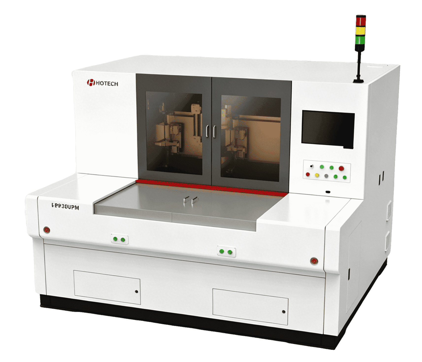
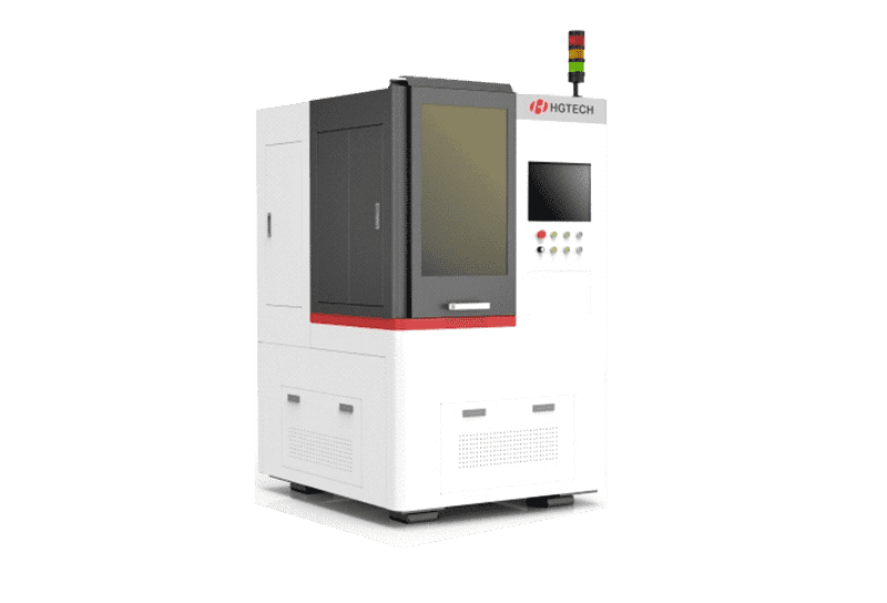
  • Picosecond UV FPC Laser Cutting

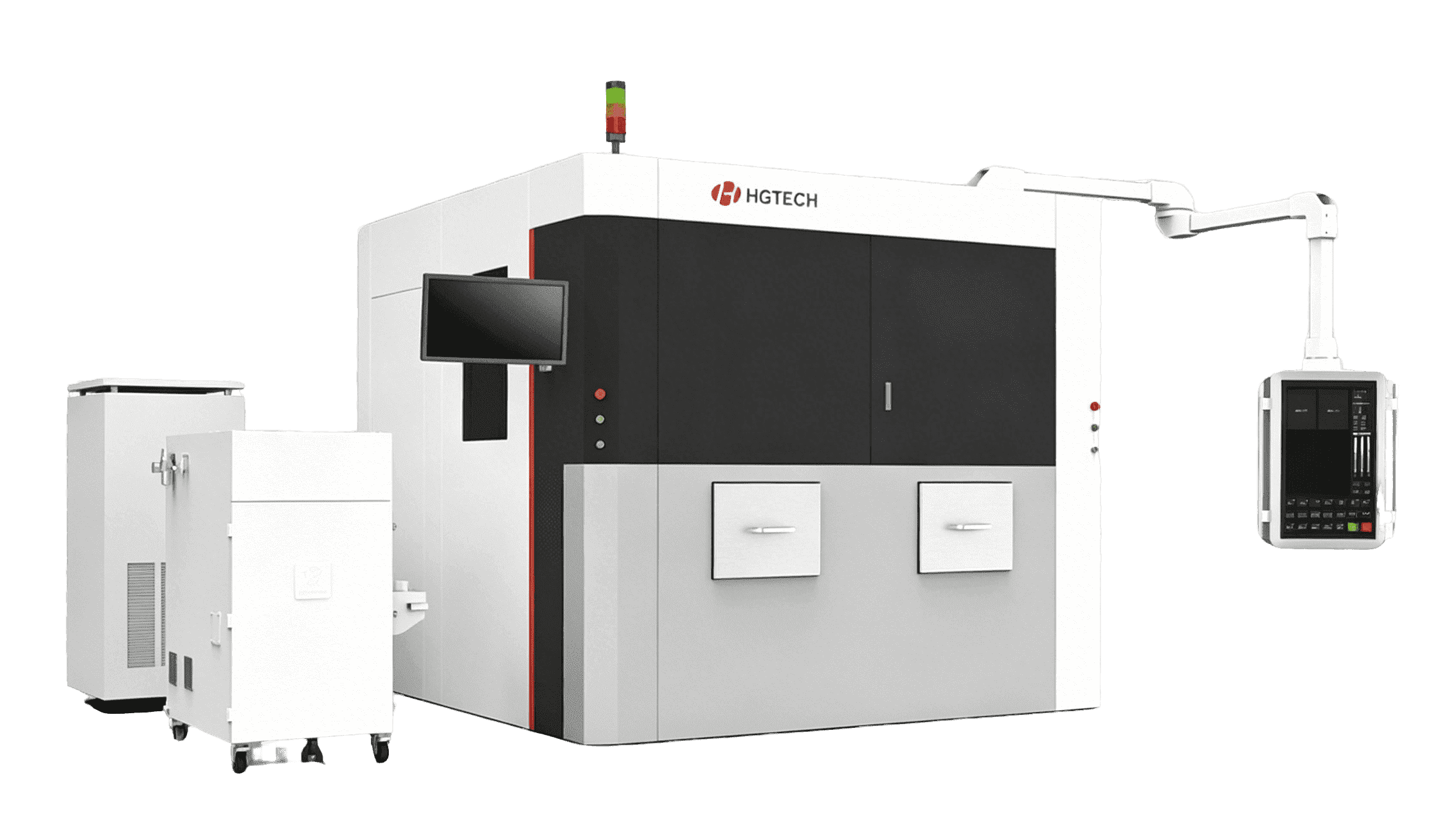
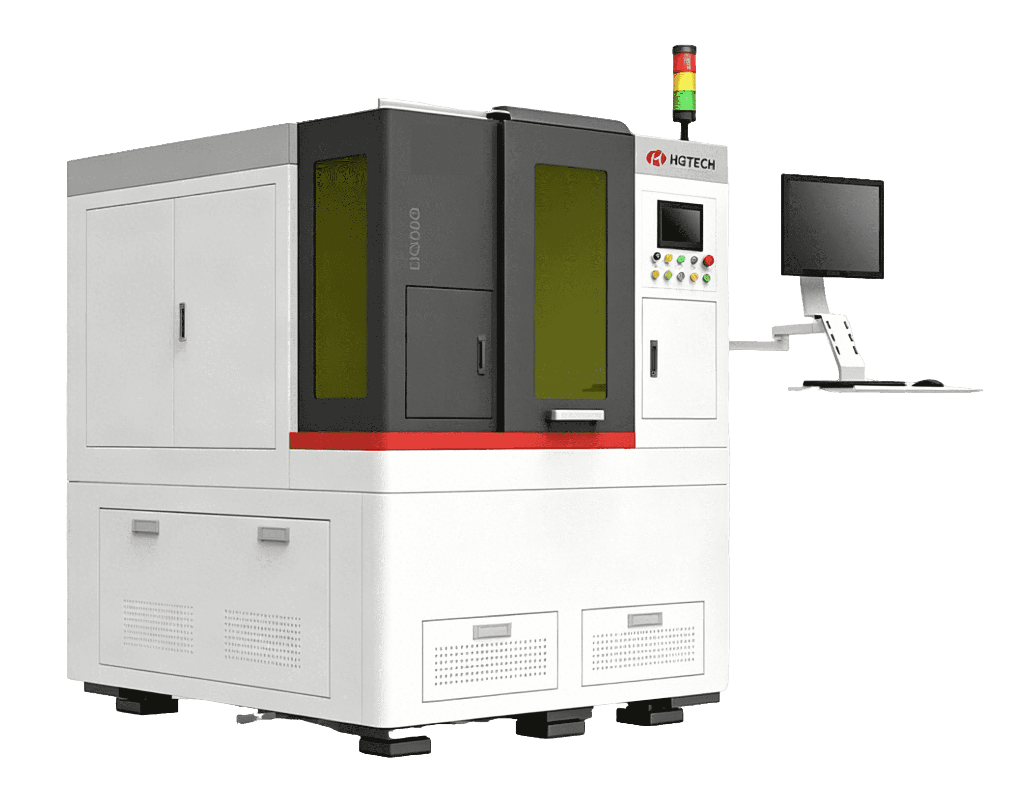
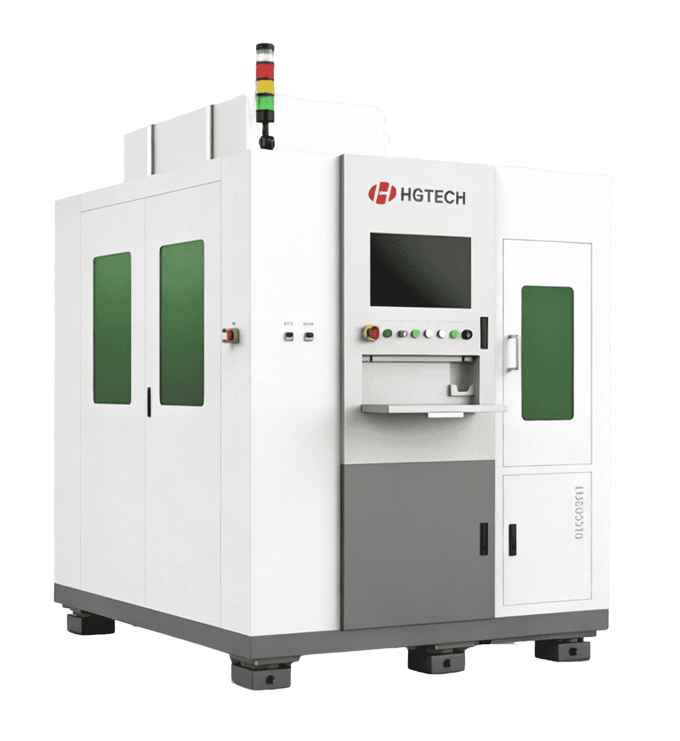
    Picosecond UV FPC laser cutting solutions are used for FPC cover film cutting, FPC shape cutting, FPC window half cutting, and RFPC cover opening.
    Value Points
    High accuracy and stability | Controlled heat-affected zone (HAZ) for consistent cutting quality | Supports no blackening and no carbonized dust requirements
    Recommended Products
    FPC Pico UV Laser Cutting Machine
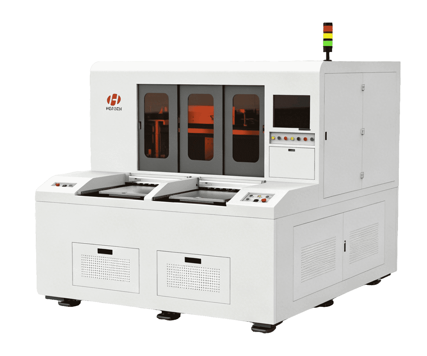
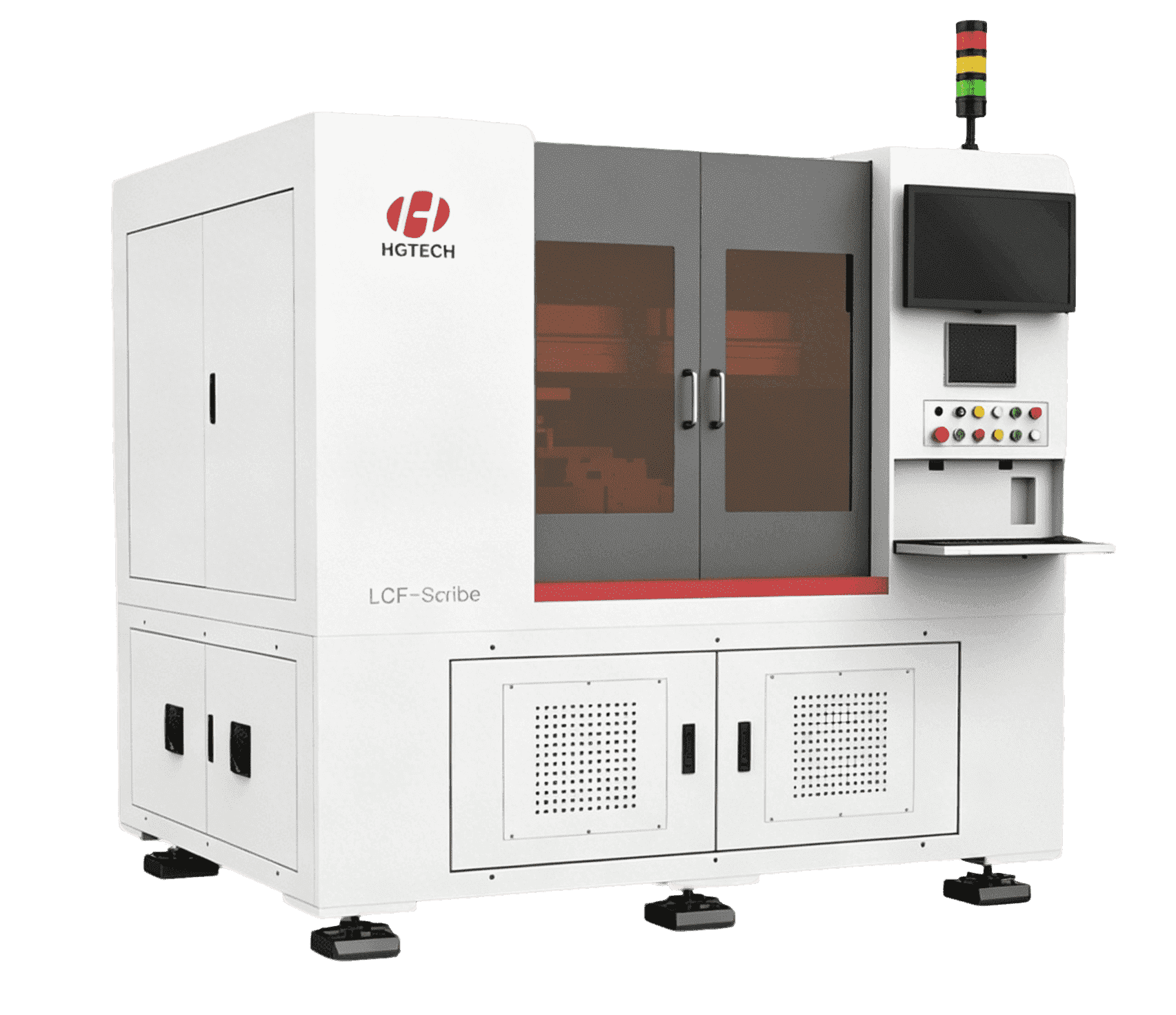
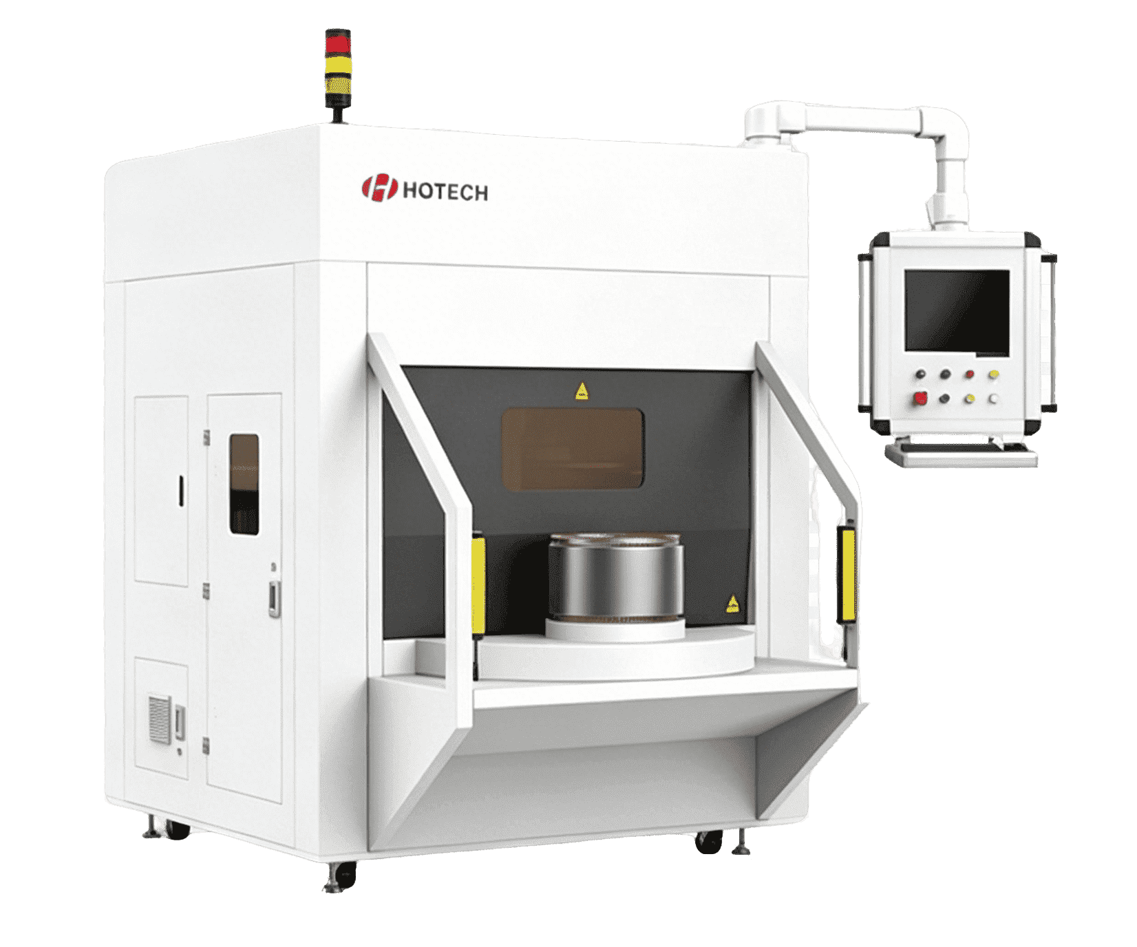
  • Ceramic Substrate Laser Cutting

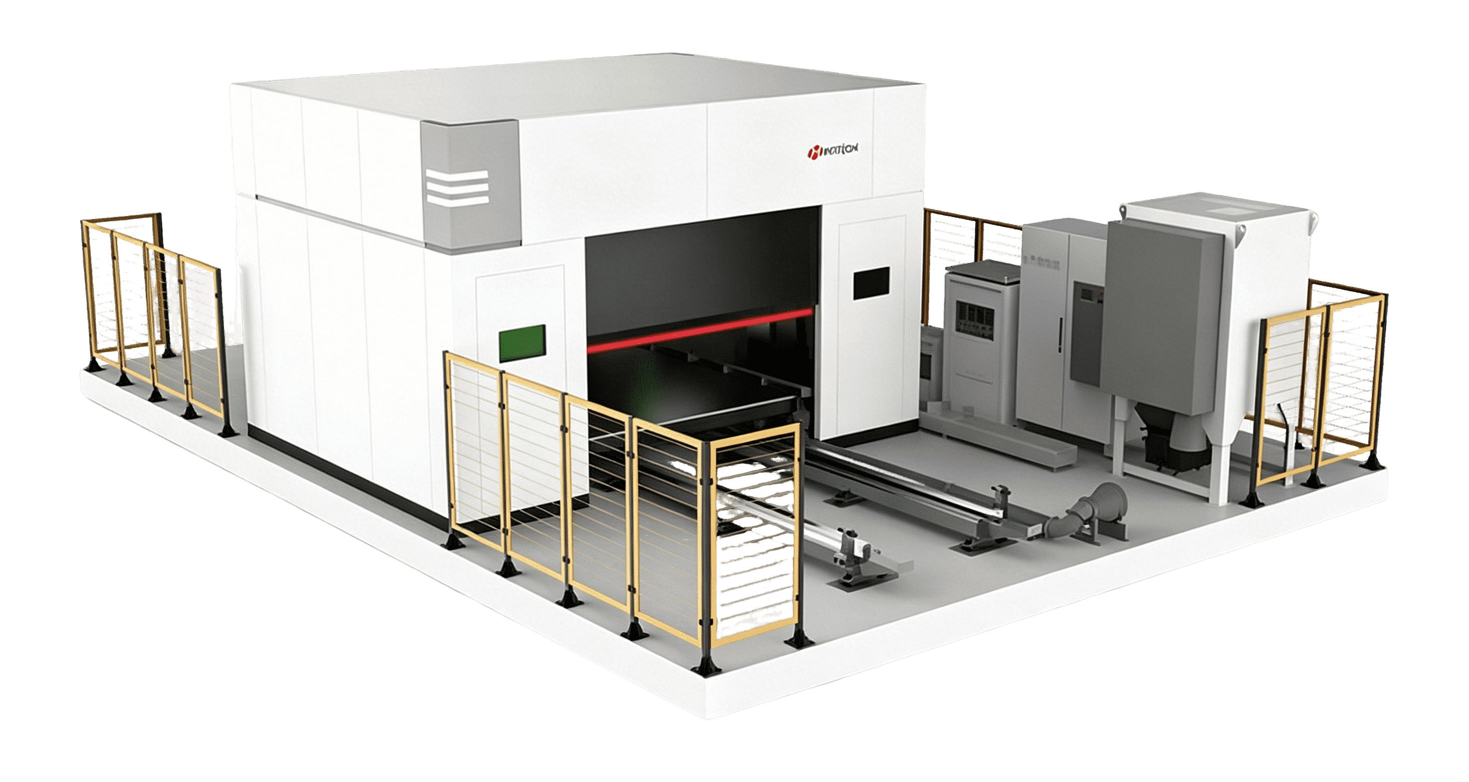
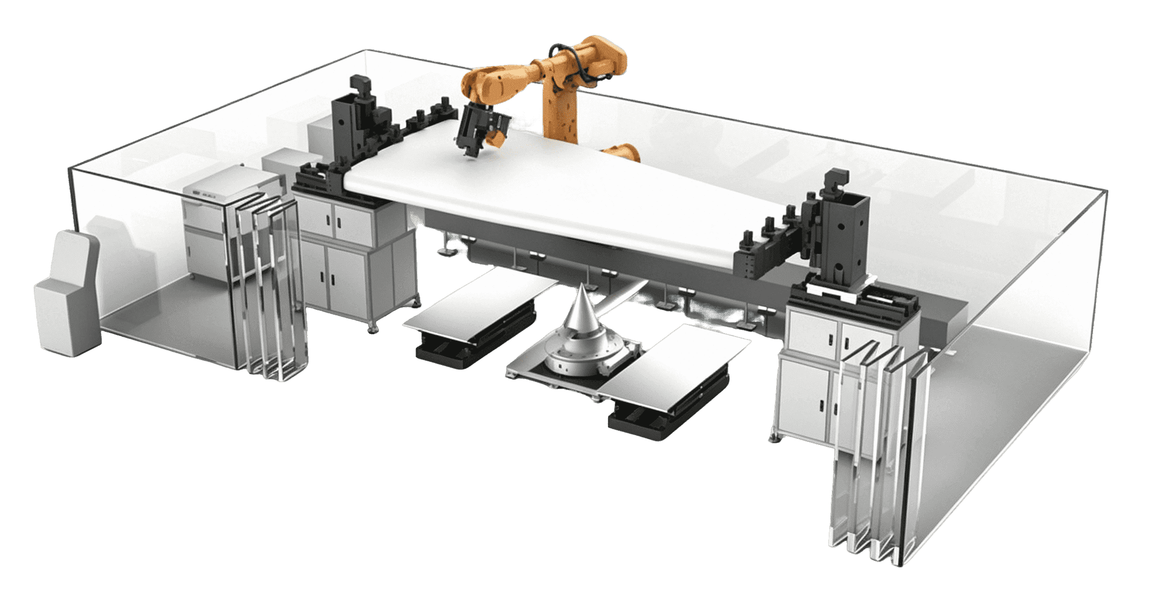
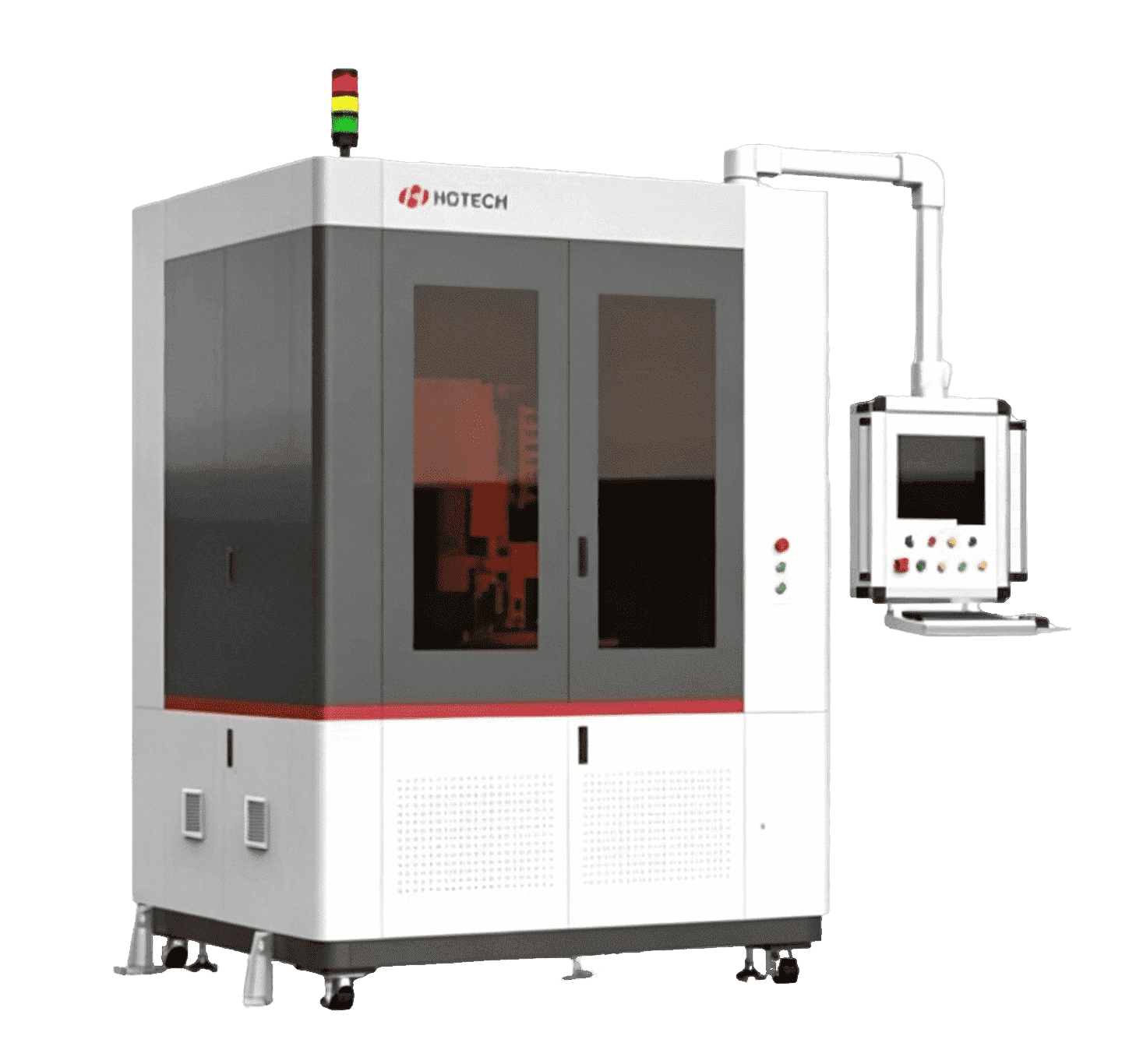
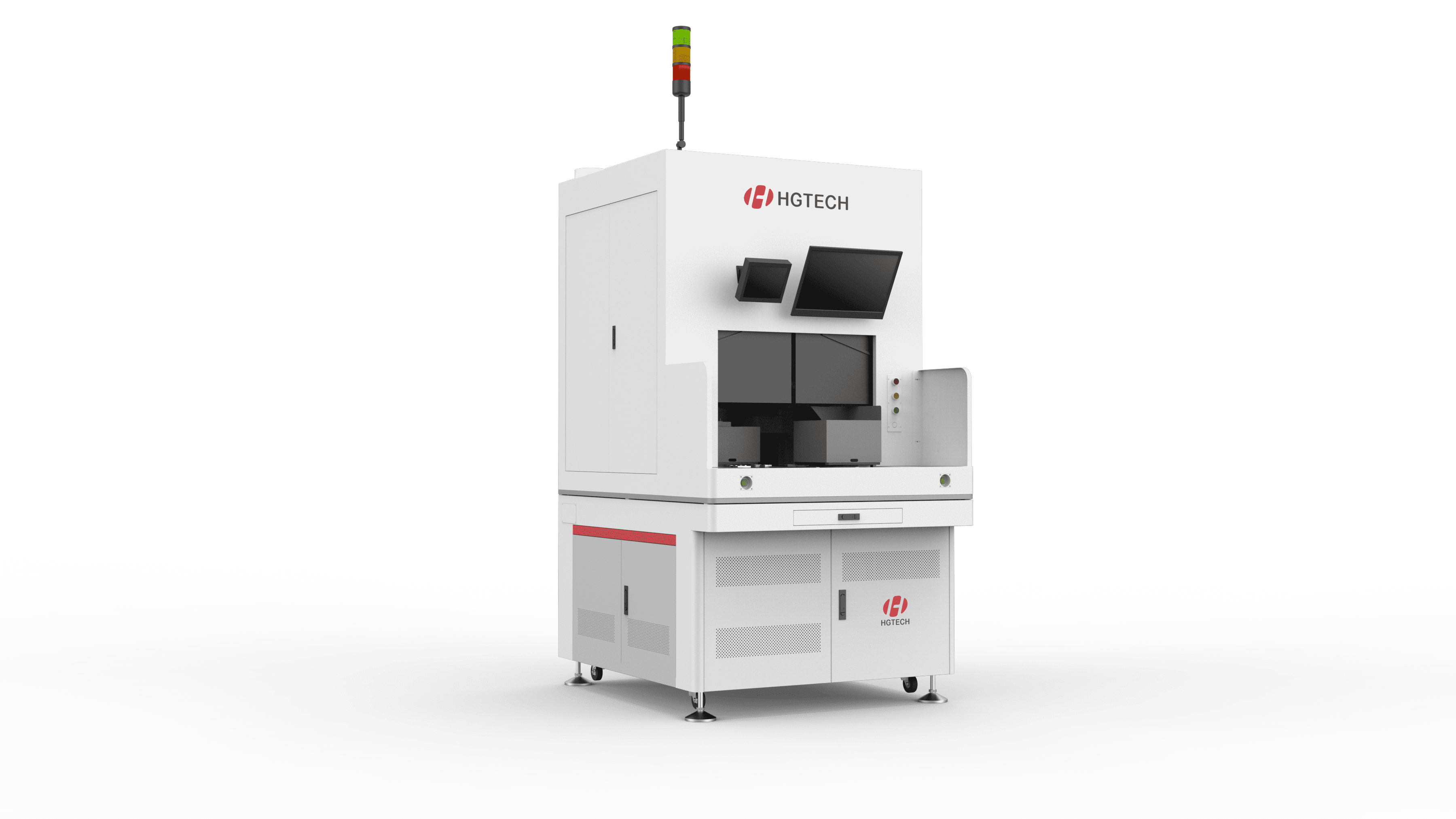
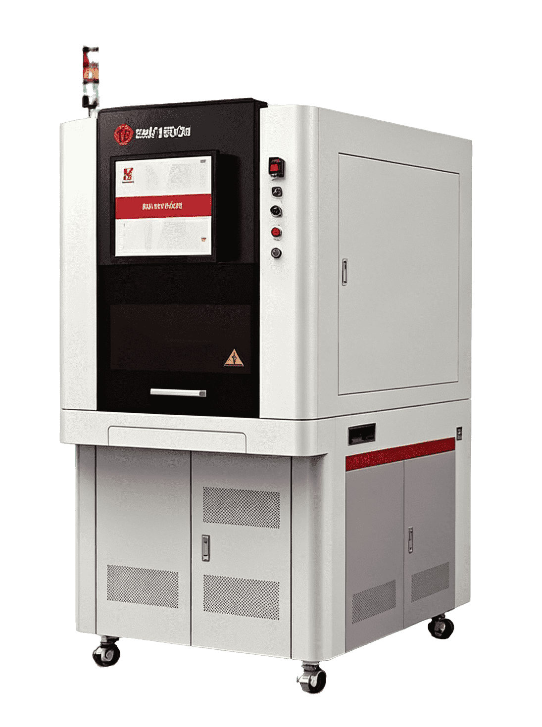
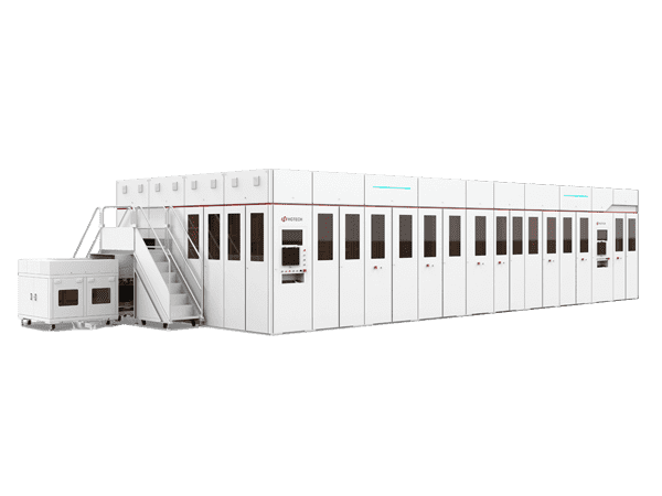
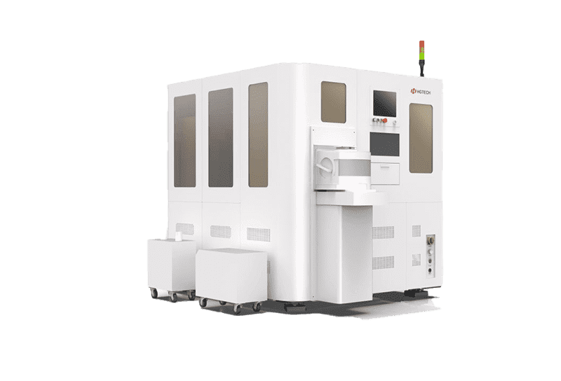
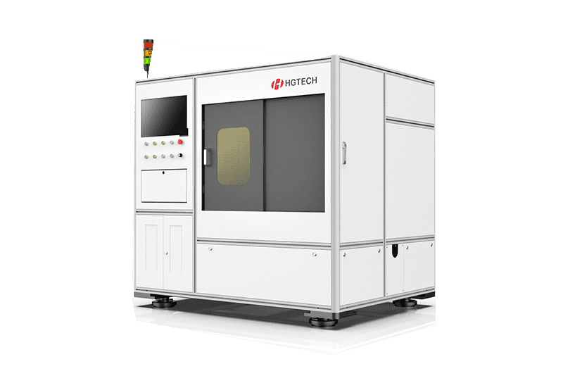
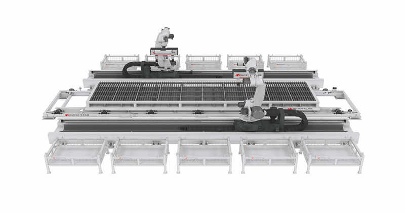
    Ceramic substrate laser cutting solutions support high-efficiency and high-precision automatic cutting for alumina, zirconium oxide, aluminum nitride, silicon nitride, and other ceramic materials.
    Value Points
    High-precision ceramic cutting | Automatic loading and unloading | Suitable for ceramic substrate processing
    Recommended Products
    Ceramic Substrate Laser Cutting Machine
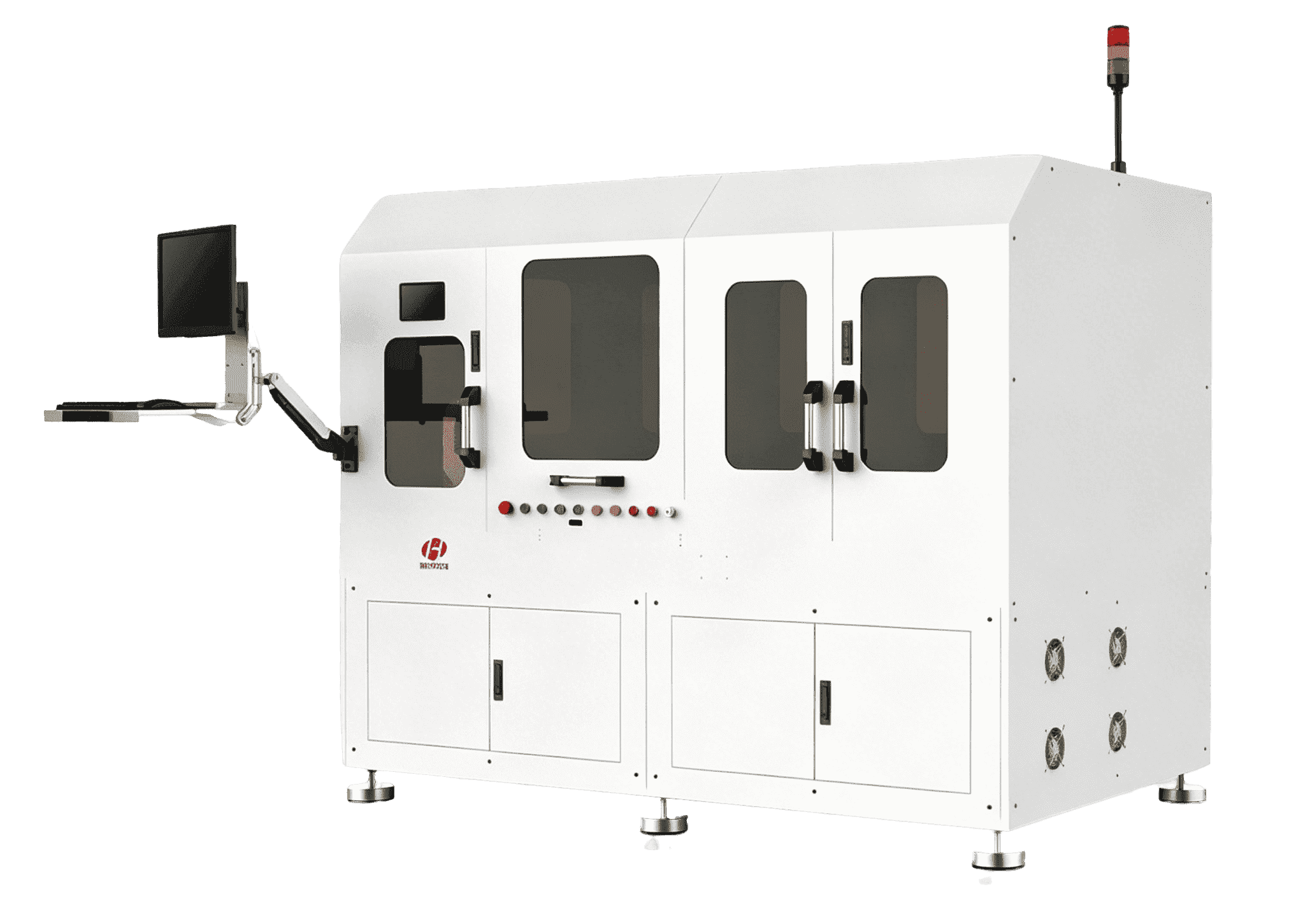
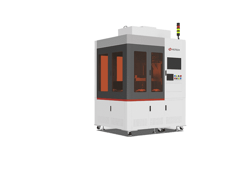
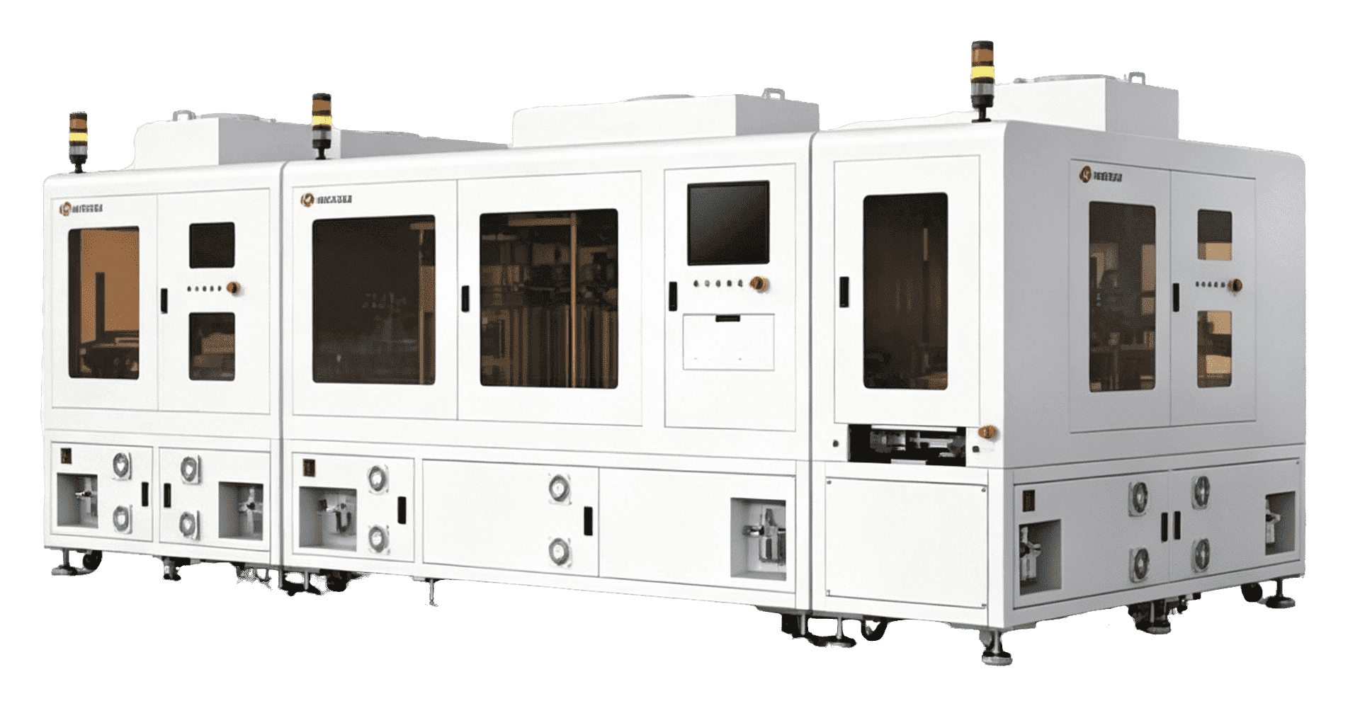
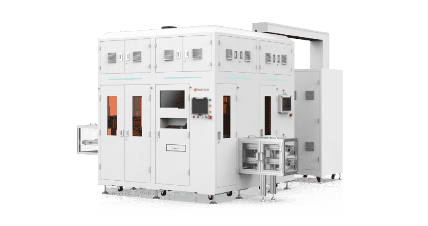
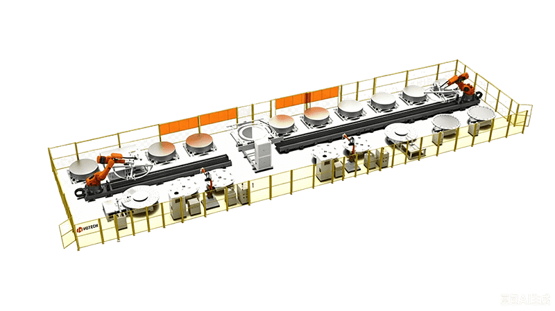
  • Fully Automated IC Packaging and Laser Marking System

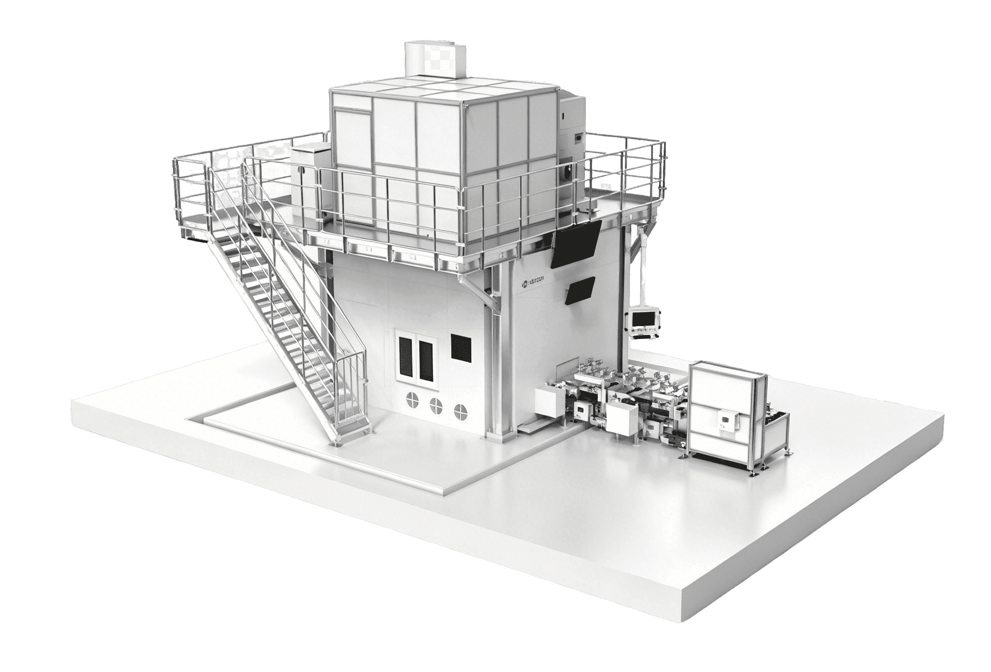
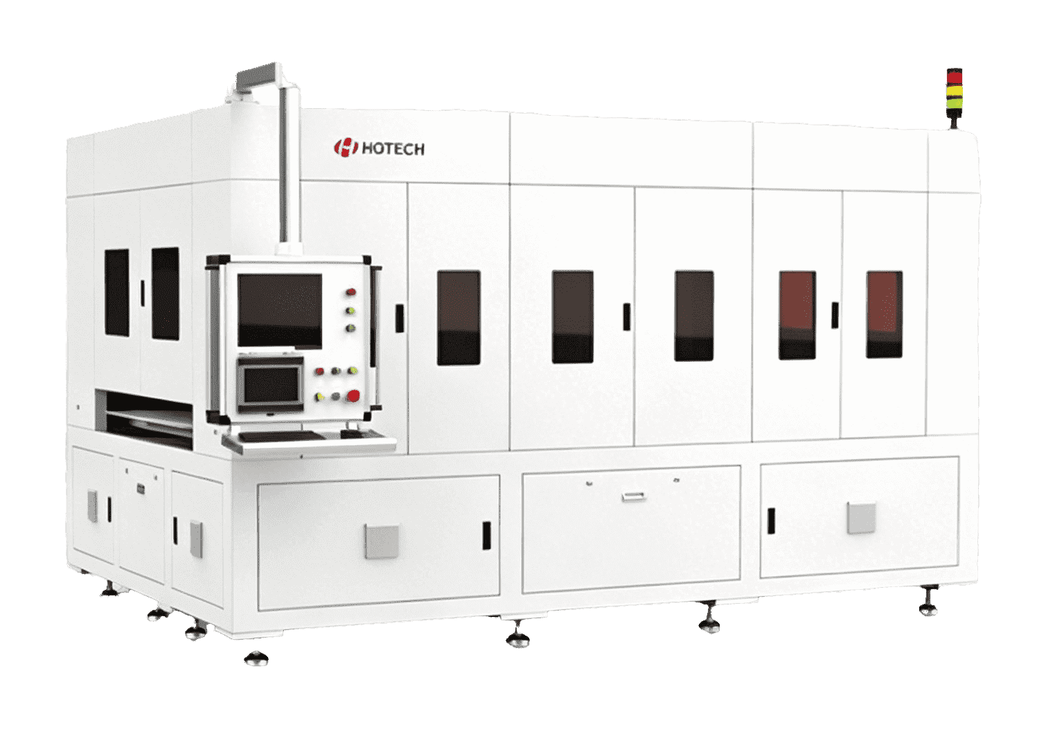
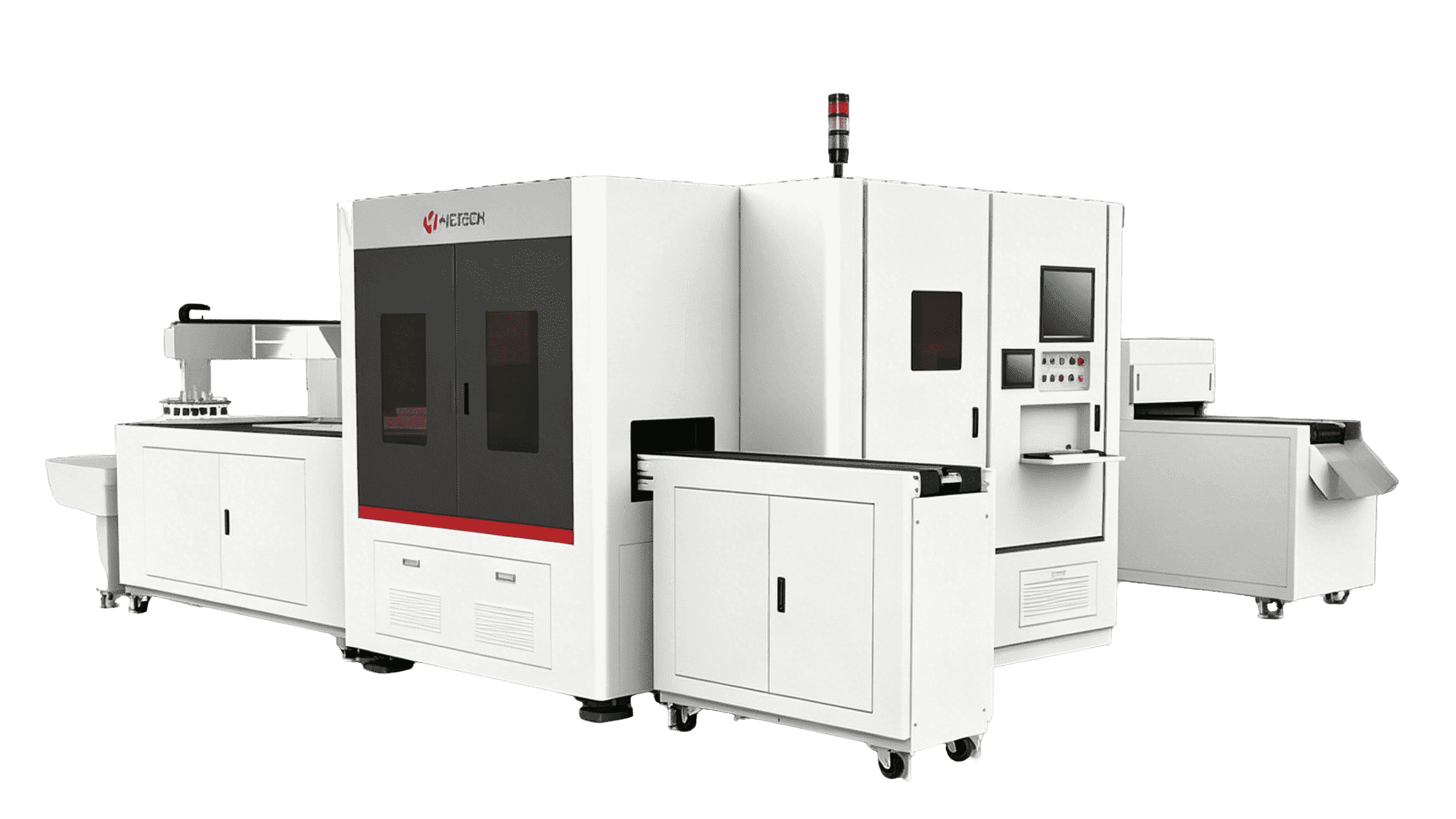
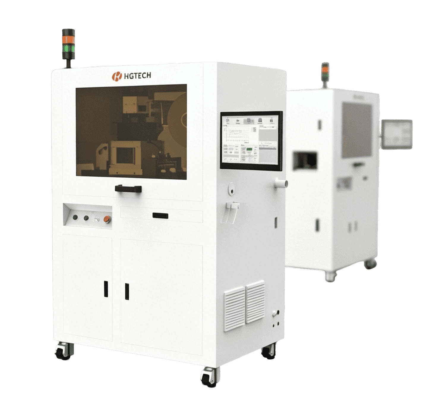
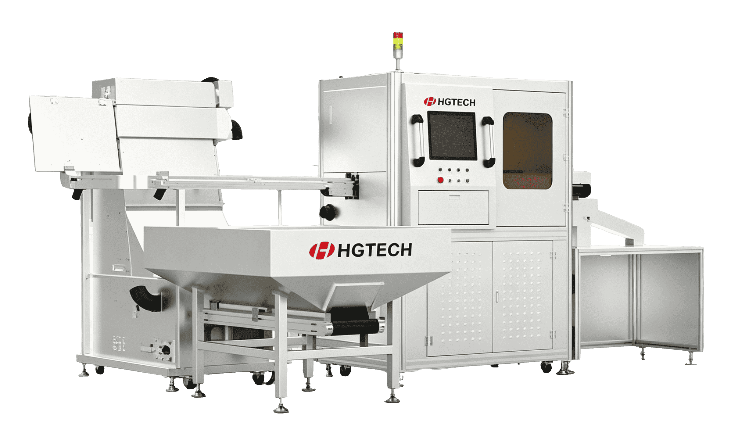
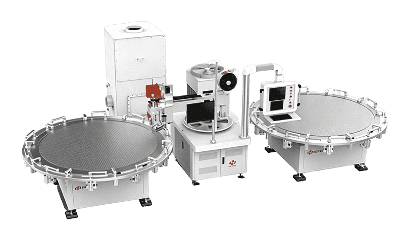
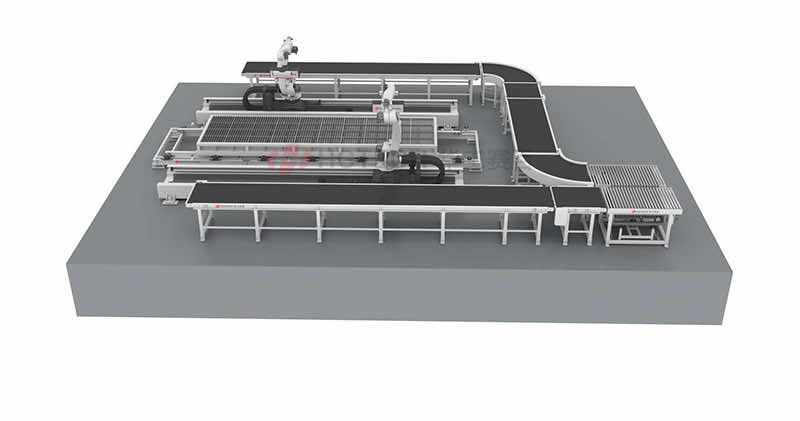
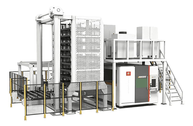
    Fully Automated IC Packaging and Laser Marking System solutions support packaged IC surface marking with automatic loading and unloading, automatic width adjustment, OCR inspection, MES data analysis, and data feedback.
    Value Points
    Automatic IC surface marking | OCR mark detection | MES data analysis and feedback
    Recommended Products
    Full-automatic IC Packaging and Laser Marking

Advanced Packaging

Glass Substrate Processing

Glass substrate processing supports micro-hole drilling, scribing, and precision cutting for advanced packaging and high-density microelectronics applications.
01

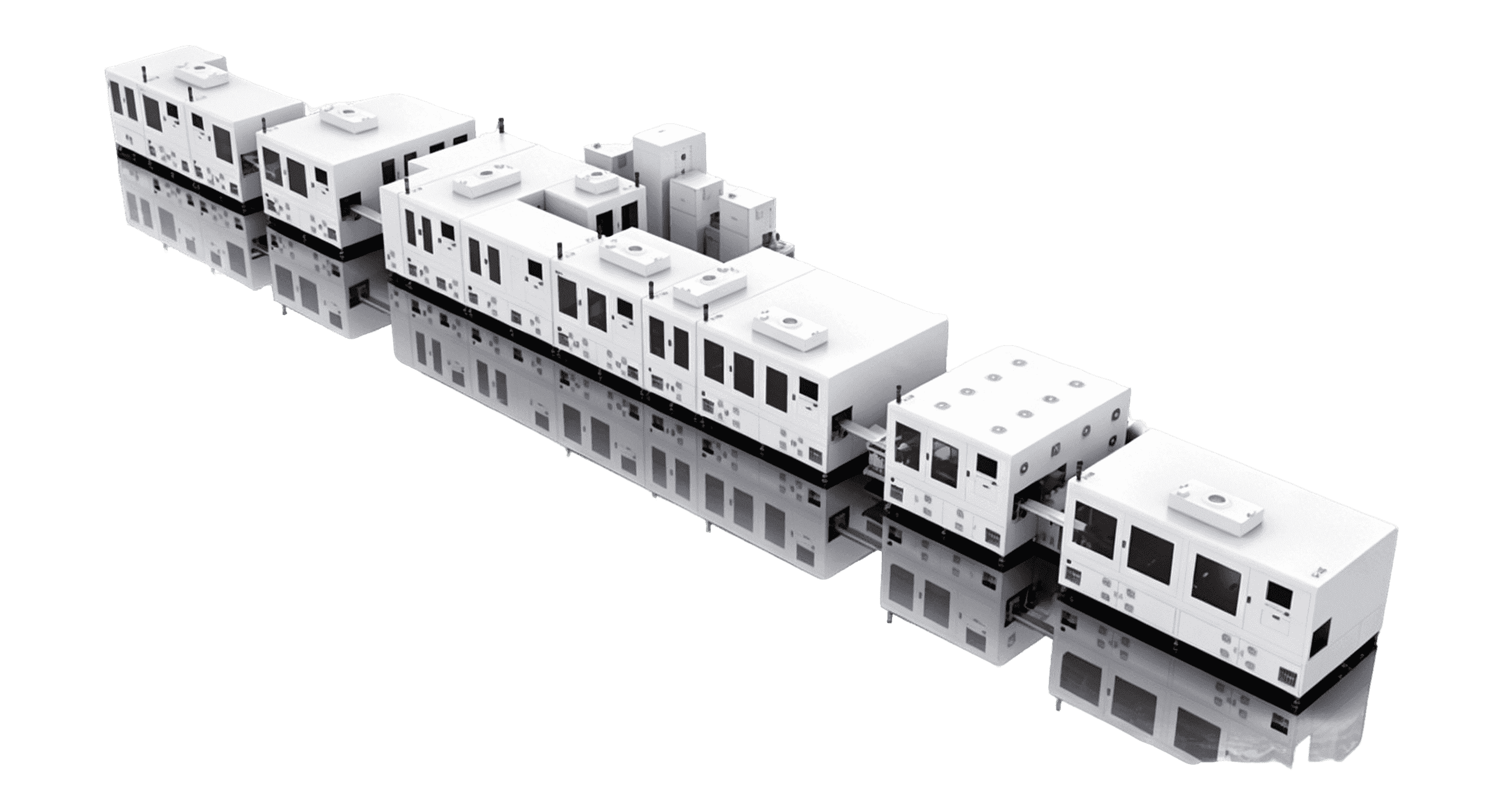
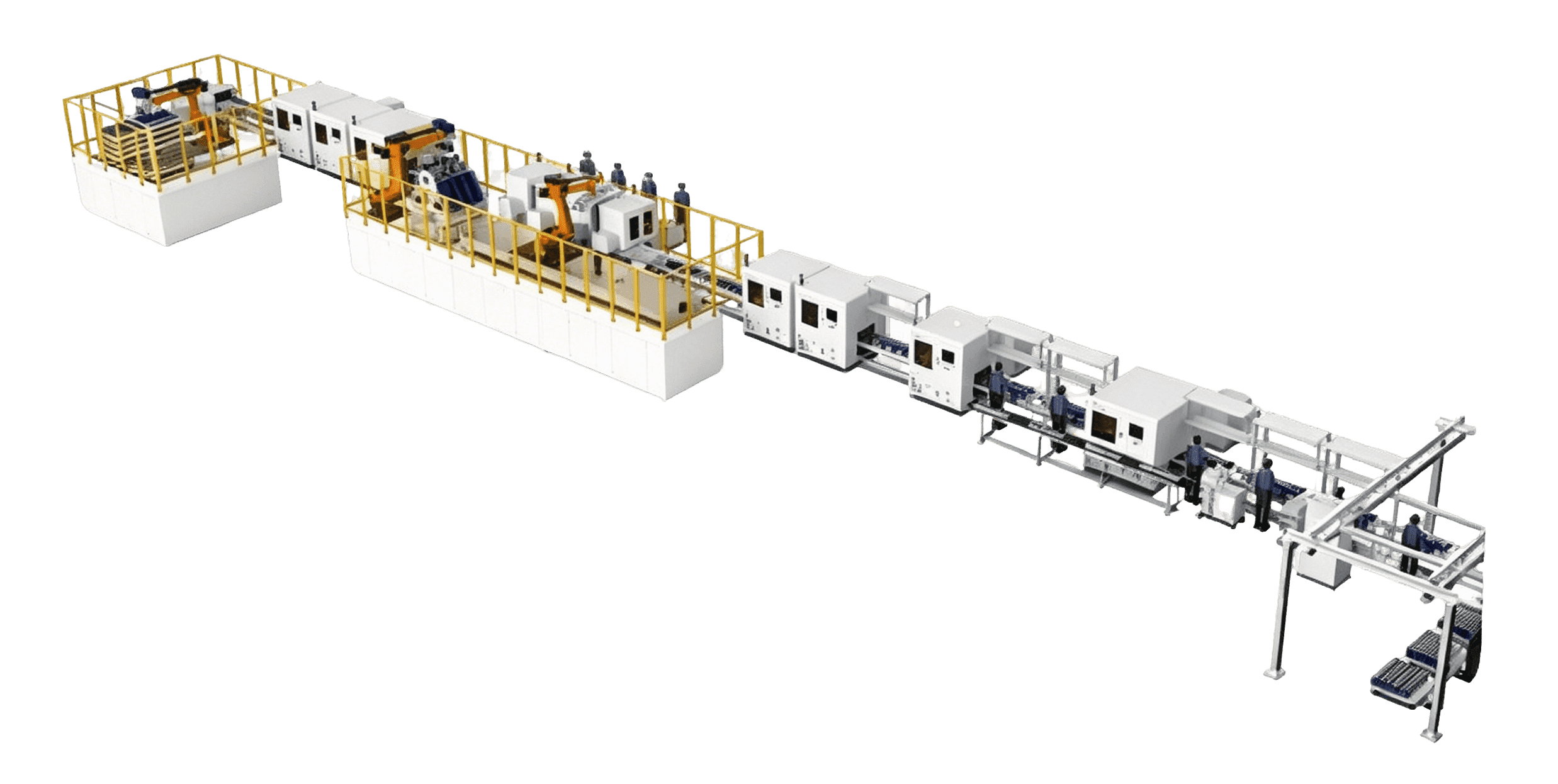
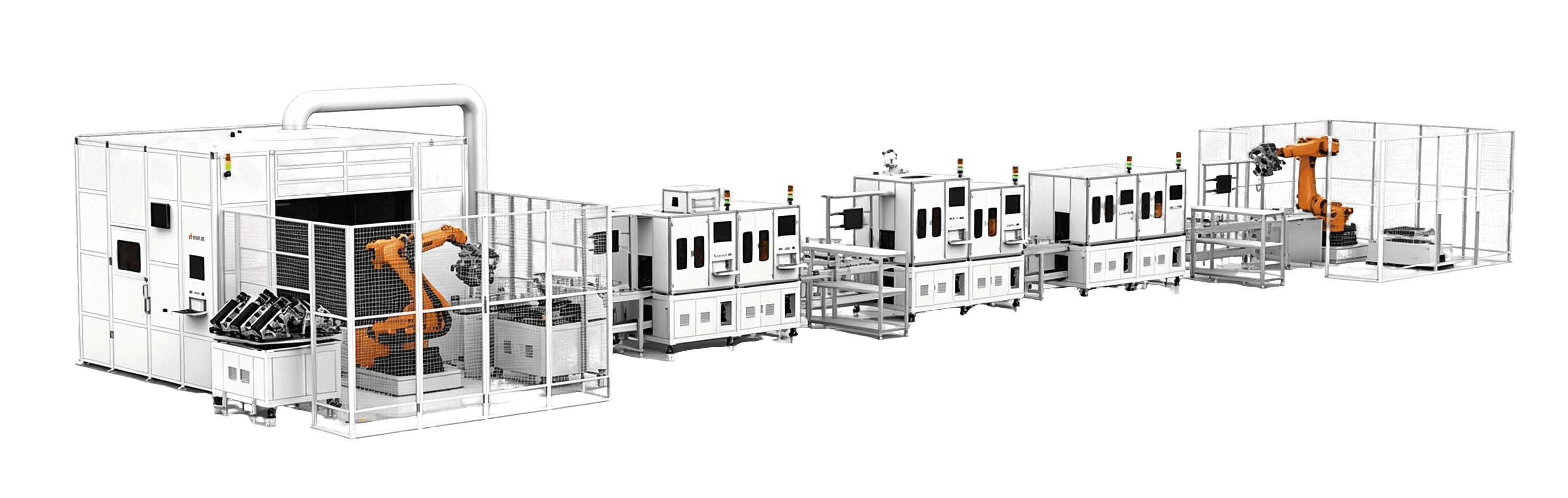
SMT and IC Substrate Laser Processing, Packaging and Inspection Solution

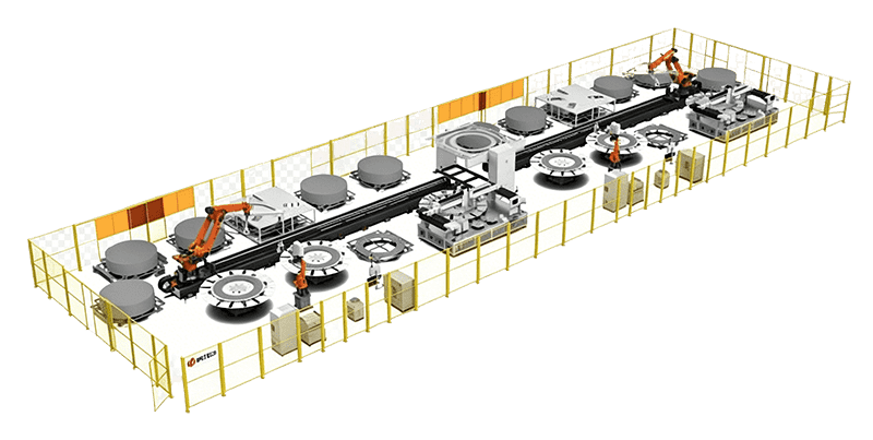
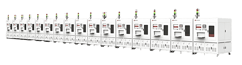
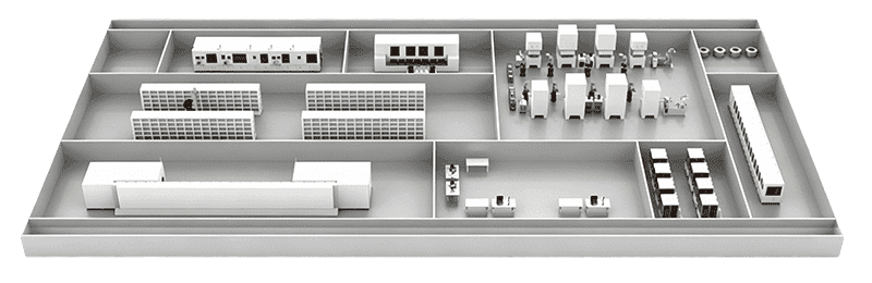
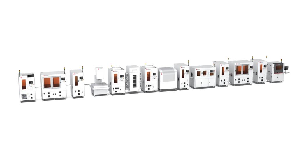
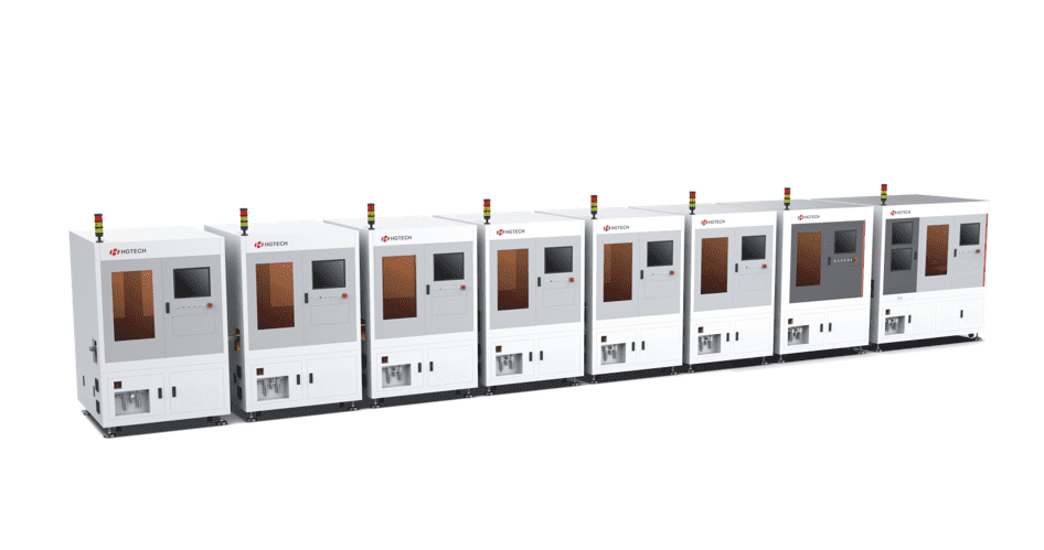
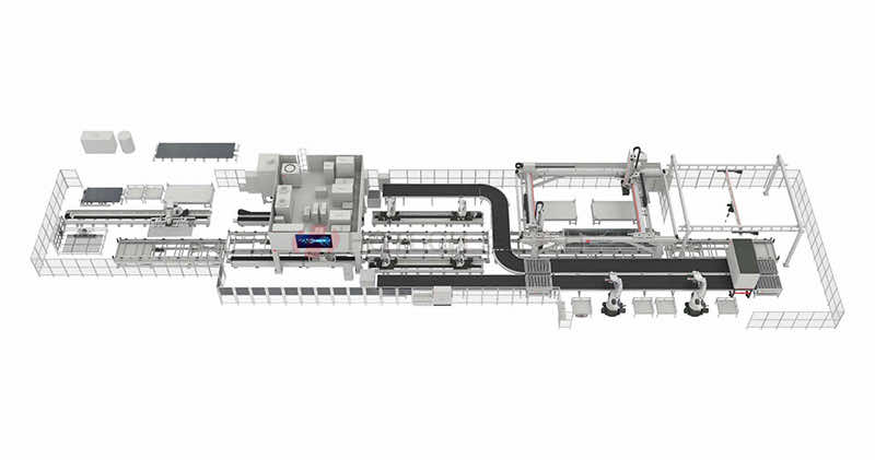
SMT and IC substrate manufacturing can be positioned around laser marking, depaneling, sorting, intelligent inspection, packaging, and traceability-oriented process integration.
Value Points
Laser processing, packaging and inspection | IC substrate process support | Traceability and quality control
Recommended Combination

· Full-automatic IC Packaging and Laser Marking Series

· IC Substrate X-Out Laser Marking Series

· SMT Double Head PCB Laser Marking Series

Smart Manufacturing
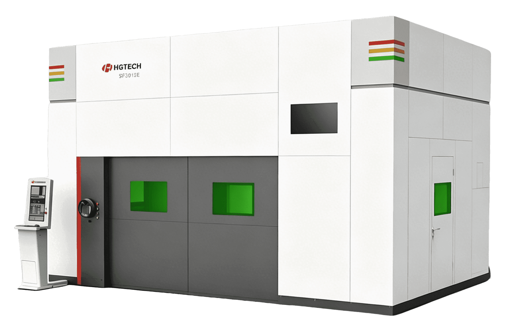
  • Laser Processing, Packaging and Inspection Support for PCB and IC Substrate Manufacturing
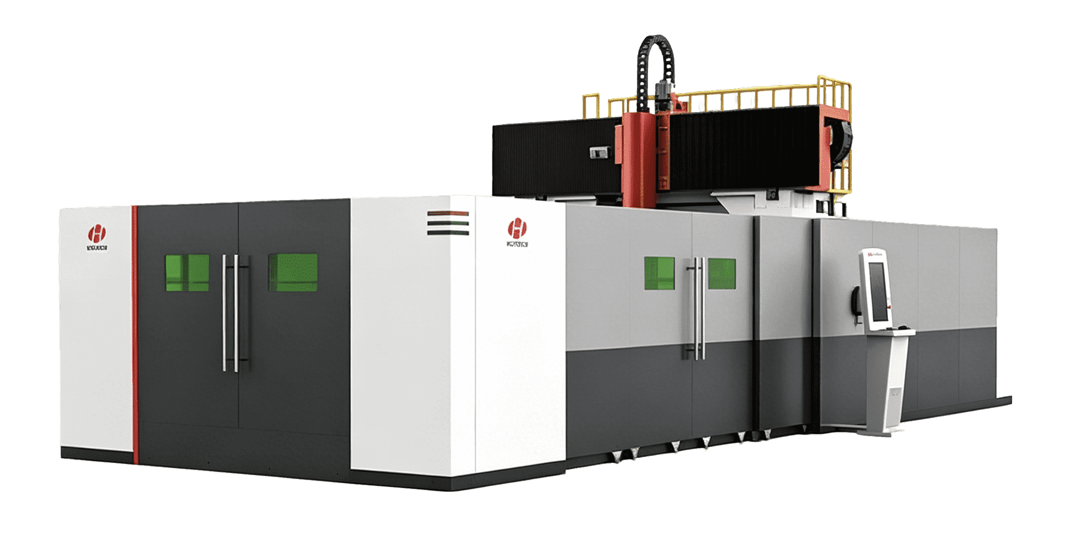
    HGTECH supports SMT and IC substrate manufacturing with laser marking, depaneling, sorting, intelligent inspection, packaging, and traceability-oriented process integration.
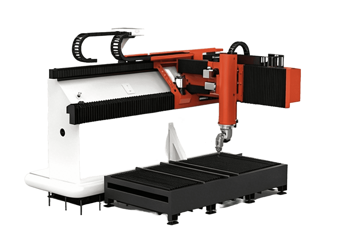
    Value Points
    Laser marking and depaneling | Intelligent inspection and packaging | Traceability-oriented process integration
    Recommended Products
    View PCB Smart Manufacturing Support
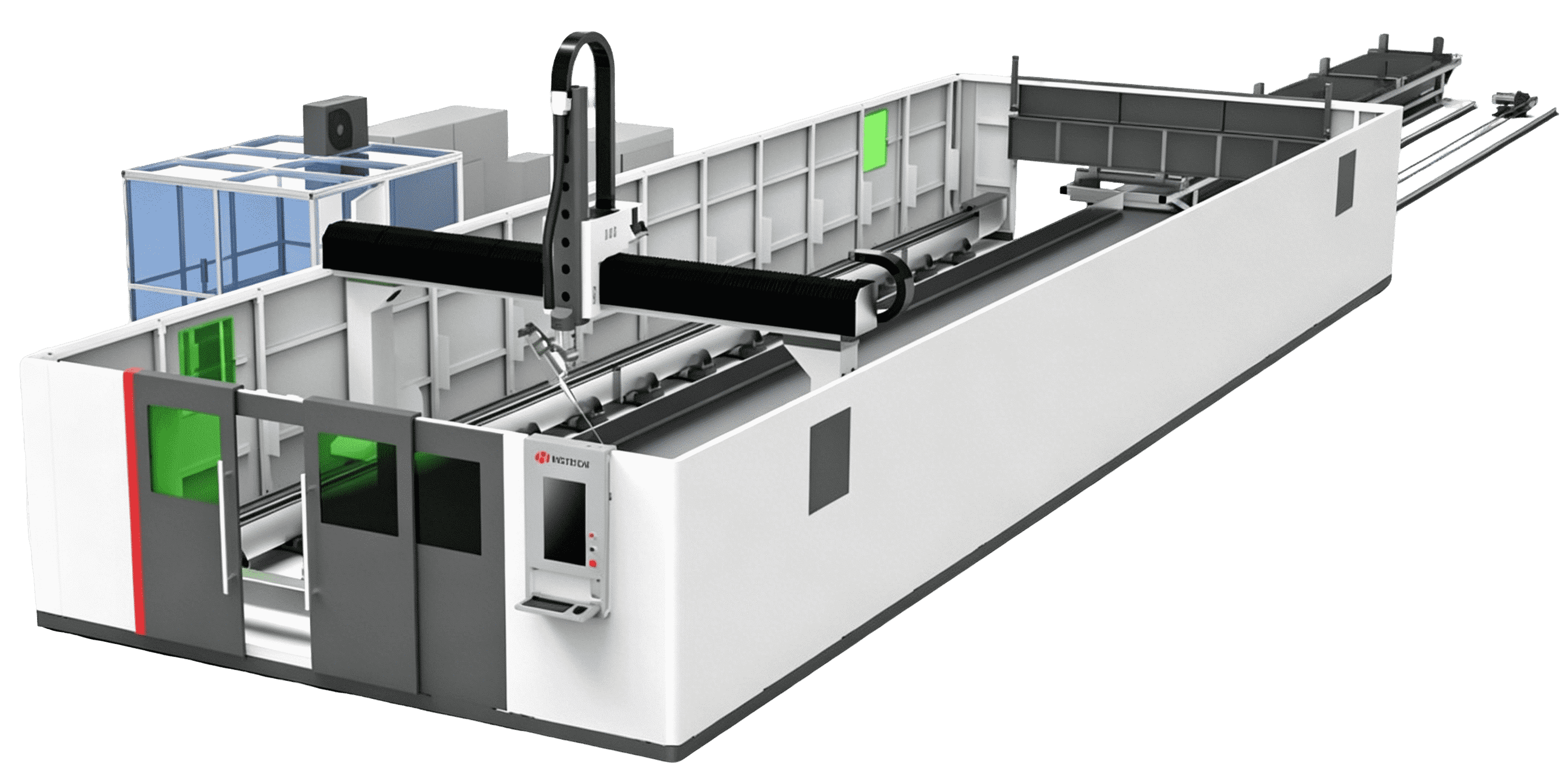
    Explore Smart Factory

Why HGTECH

Integrated capabilities for PCB and microelectronics manufacturing
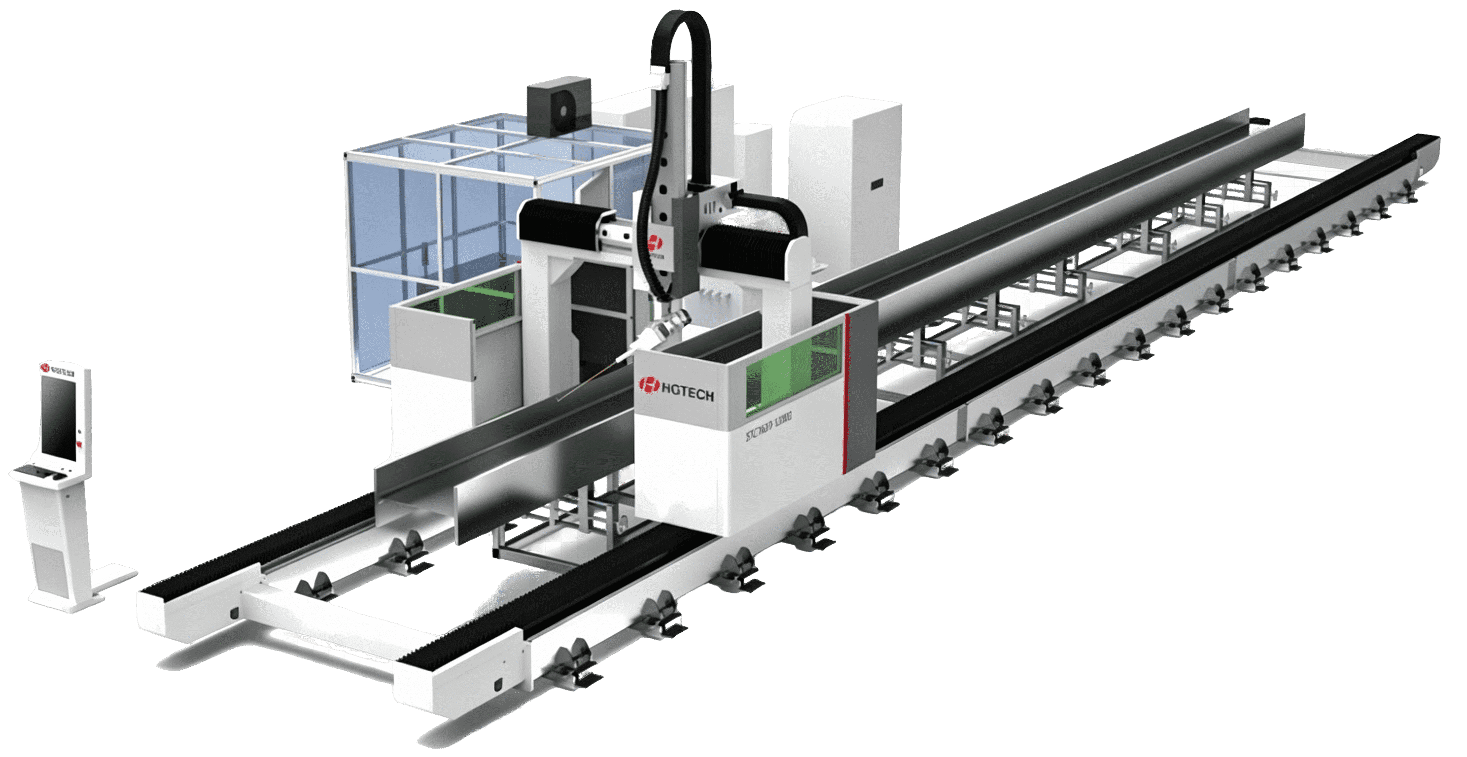
HGTECH combines precision laser processing equipment, automation modules, inspection support, and traceability-oriented manufacturing capabilities for PCB and microelectronics production.
  • Precision Laser Processing

  • SMT/IC Substrate Automation

  • Traceability and Inspection Support

Innovation Capability

  • 12
    National-Level Talent & Technology Platforms
  • 100+
    Scientific Research Achievement Awards
  • 3000+
    Independent Intellectual Property Rights

Innovative Achievements

  • In 2015, the project "Key Technologies and Complete Equipment for High-quality and High-efficiency Laser Welding and Cutting in Automobile Manufacturing" won the First Prize of the National Award for Progress in Science and Technology.
  • Since its establishment, it has obtained more than 100 national, provincial and ministerial scientific research achievement awards, including 4 National Awards for Progress in Science and Technology.
  • It has achieved over 70 "China’s Firsts" in the industry.
  • The average annual growth rate of authorized patents exceeded 28% in the past five years.
  • Led the formulation of the first international standard for China’s laser industry.
  • The average annual sales contribution rate of new products reached 41% over the past five years.
  • The National Enterprise Technology Center ranked 123rd among 1,744 evaluated institutions nationwide, topping the industry.

Discuss PCB and microelectronics laser processing solutions

Connect with our team to explore laser depaneling, marking, drilling, cutting, IC substrate, ceramic substrate, and smart manufacturing solutions for PCB and microelectronics applications.